|
Absolute Max. Rating |
Recommended working conditions |
|
Input voltage:400V Output power:500W Storage temperature:-55~125℃ Lead resistance to welding temperature(10s):less than300℃ Junction temperature:less than150℃ |
Input voltage:180~375V Operating temperature(Tc):-55~100℃ |
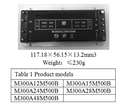
Table 3a Electrical characteristics of M300A12M500B
|
NO. |
Items |
Symbol |
Unless otherwise specified -55℃≤Tc≤100℃, VIN=270V±10V |
Limit value |
Unit |
||
|
Min |
Max |
||||||
|
1 |
Input voltage/V |
Turn on voltage |
VINL-ONT
VINL-OFF |
|
- |
178.2 |
V |
|
Turn off voltage |
147.4 |
- |
V |
||||
|
2 |
Insulation resistance |
Riso |
TA=25℃,Input, bottom plate and output between any two plus 1000V(DC) |
100 |
- |
MΩ |
|
|
3 |
Output voltage |
Vo |
TA=25℃,Full load |
11.88 |
12.12 |
V |
|
|
4 |
Output current |
Io |
Full load |
|
41.6 |
A |
|
|
5 |
Voltage regulation |
Sv |
180V~375V,Full load |
- |
1 |
% |
|
|
6 |
Load regulation |
S1 |
10% load~full load |
- |
1 |
% |
|
|
7 |
Temperature coefficient |
av |
Full load |
- |
0.02 |
%/℃ |
|
|
8 |
Effectiveness |
η |
TA=25℃,Full load TA=-55℃,Tc=100℃, Full load |
85 |
- |
% |
|
|
83 |
- |
% |
|||||
|
9 |
Ripple and noise voltage(Peak-peak) |
VR |
TA=25℃,Band width≤20MHz,Full load |
- |
350 |
mV |
|
|
TA=-55℃,Tc=100℃, Band width≤20MHz,Full load |
- |
700 |
mV |
||||
|
10 |
SC Reference voltage |
Vb-SC |
TA=25℃,Relative to the negative induction |
1.21 |
1.25 |
V |
|
|
11 |
Short circuit protection current |
|
TA=25℃ |
15 |
mA |
||
|
12 |
PC side disabled function |
|
TA=25℃,50% load |
- |
2 |
V |
|
|
13 |
Power distribution accuracya |
PE |
TA=25℃,full load |
- |
5 |
% |
|
|
14 |
Output over voltage protection pointa |
VOVP |
TA=25℃,50% load |
13.7 |
14.9 |
V |
|
|
15 |
Output voltage adjustment rangea |
VTR |
TA=25℃,50% load |
90 |
110 |
% |
|
|
16 |
Inductive compensation voltagea |
VSC |
Each terminal less than 0.25V(Sensing end closed) |
- |
0.5 |
V |
|
|
a Design assurance,Only test when the inspection is carried out or when the design process change affecting the parameters。 |
|||||||
Table 3b Electrical characteristics of M300A15M500B
|
NO. |
Items |
Symbol |
Unless otherwise specified -55℃≤Tc≤100℃, VIN=270V±10V |
Limit value |
Unit |
||
|
Min |
Max |
||||||
|
1 |
Input voltage/V |
Turn on voltage |
VINL-ONT
VINL-OFF |
|
- |
178.2 |
V |
|
Turn off voltage |
147.4 |
- |
V |
||||
|
2 |
Insulation resistance |
Riso |
TA=25℃,Input, bottom plate and output between any two plus 1000V(DC) |
100 |
- |
MΩ |
|
|
3 |
Output voltage |
Vo |
TA=25℃,Full load |
14.85 |
15.15 |
V |
|
|
4 |
Output current |
Io |
Full load |
|
33.3 |
A |
|
|
5 |
Voltage regulation |
Sv |
180V~375V,Full load |
- |
1 |
% |
|
|
6 |
Load regulation |
S1 |
10% load~full load |
- |
1 |
% |
|
|
7 |
Temperature coefficient |
av |
Full load |
- |
0.02 |
%/℃ |
|
|
8 |
Effectiveness |
η |
TA=25℃,Full load TA=-55℃,Tc=100℃, Full load |
84 |
- |
% |
|
|
82 |
- |
% |
|||||
|
9 |
Ripple and noise voltage(Peak-peak) |
VR |
TA=25℃,Band width≤20MHz,Full load |
- |
250 |
mV |
|
|
TA=-55℃,Tc=100℃, Band width≤20MHz,Full load |
- |
500 |
mV |
||||
|
10 |
SC Reference voltage |
Vb-SC |
TA=25℃,Relative to the negative induction |
1.21 |
1.25 |
V |
|
|
11 |
Short circuit protection current |
|
TA=25℃ |
15 |
mA |
||
|
12 |
PC side disabled function |
|
TA=25℃,50% load |
- |
2 |
V |
|
|
13 |
Power distribution accuracya |
PE |
TA=25℃,full load |
- |
5 |
% |
|
|
14 |
Output over voltage protection pointa |
VOVP |
TA=25℃,50% load |
17.1 |
18.5 |
V |
|
|
15 |
Output voltage adjustment rangea |
VTR |
TA=25℃,50% load |
90 |
110 |
% |
|
|
16 |
Inductive compensation voltagea |
VSC |
Each terminal less than 0.25V(Sensing end closed) |
- |
0.5 |
V |
|
|
a Design assurance,Only test when the inspection is carried out or when the design process change affecting the parameters. |
|||||||
Table 3c Electrical characteristics of M300A24M500B
|
NO. |
Items |
Symbol |
Unless otherwise specified -55℃≤Tc≤100℃, VIN=270V±10V |
Limit value |
Unit |
||
|
Min |
Min |
||||||
|
1 |
Input voltage/V |
Turn on voltage |
VINL-ONT
VINL-OFF |
|
- |
178.2 |
V |
|
Turn off voltage |
147.4 |
- |
V |
||||
|
2 |
Insulation resistance |
Riso |
TA=25℃,Input, bottom plate and output between any two plus 1000V(DC) |
100 |
- |
MΩ |
|
|
3 |
Output voltage |
Vo |
TA=25℃,Full load |
23.76 |
24.24 |
V |
|
|
4 |
Output current |
Io |
Full load |
|
20.8 |
A |
|
|
5 |
Voltage regulation |
Sv |
180V~375V,Full load |
- |
1 |
% |
|
|
6 |
Load regulation |
S1 |
10% load~full load |
- |
1 |
% |
|
|
7 |
Temperature coefficient |
av |
Full load |
- |
0.02 |
%/℃ |
|
|
8 |
Effectiveness |
η |
TA=25℃,Full load TA=-55℃,Tc=100℃, Full load |
87 |
- |
% |
|
|
85 |
- |
% |
|||||
|
9 |
Ripple and noise voltage(Peak-peak) |
VR |
TA=25℃,Band width≤20MHz,Full load |
- |
125 |
mV |
|
|
TA=-55℃,Tc=100℃, Band width≤20MHz,Full load |
- |
250 |
mV |
||||
|
10 |
SC Reference voltage |
Vb-SC |
TA=25℃,Relative to the negative induction |
1.21 |
1.25 |
V |
|
|
11 |
Short circuit protection current |
|
TA=25℃ |
Flow reduction type |
|
||
|
12 |
PC side disabled function |
|
TA=25℃,50% load |
- |
2 |
V |
|
|
13 |
Power distribution accuracya |
PE |
TA=25℃,full load |
- |
5 |
% |
|
|
14 |
Output over voltage protection pointa |
VOVP |
TA=25℃,50% load |
27.1 |
29.1 |
V |
|
|
15 |
Output voltage adjustment rangea |
VTR |
TA=25℃,50% load |
90 |
110 |
% |
|
|
16 |
Inductive compensation voltagea |
VSC |
Each terminal less than 0.25V(Sensing end closed) |
- |
0.5 |
V |
|
|
a Design assurance,Only test when the inspection is carried out or when the design process change affecting the parameters. |
|||||||


|
Pin |
Symbol |
Designation |
|
1 |
+In |
Positive Input |
|
2 |
PC |
Inhibit and alarm |
|
3 |
PR |
Parallel |
|
4 |
- In |
Negative Input |
|
5 |
- Out |
Negative Output |
|
6 |
- S |
Negative Induction |
|
7 |
SC |
Secondary control |
|
8 |
+ S |
Positive Induction |
|
9 |
+Out |
Positive Output |


|
Symbols |
Unit/mm |
||
|
Minimum |
Typical |
Minimum |
|
|
A |
12.20 |
- |
13.50 |
|
A1 |
2.80 |
- |
3.30 |
|
A2 |
10.65 |
- |
11.40 |
|
Φb1 |
4.44 |
- |
4.70 |
|
Φb2 |
1.90 |
- |
2.16 |
|
D |
116.42 |
- |
117.18 |
|
E |
43.95 |
- |
44.95 |
|
e2 |
- |
17.78 |
- |
|
e3 |
- |
7.62 |
- |
|
e1 |
- |
106.68 |
- |
|
L |
|
4.58 |
- |
|
X1 |
45.45 |
- |
45.95 |
|
Y1 |
50.55 |
- |
51.05 |
|
d |
3.17 |
- |
3.55 |
|
Y |
55.65 |
- |
56.15 |


Subscribe to our weekly newsletter and receive exclusive offers on products you love!
 X
X


 Gold Supplier