|
MODELS |
|
|
SINGLE |
DUAL |
|
HHF28S3R3(F) HHF28S5(F) HHF28S5R2(F) HHF28S12(F) HHF28S15(F) HHF28S28(F) HHF28S08(F) |
HHF28D5(F) HHF28D12(F) HHF28D15(F) HHF28D5N HHF28D6N HHF28D12N HHF28D15N |
| Single output models | HHF28S5(F) | HHF28S12(F) | HHF28S15(F) | |||||||
| Parameter | Conditions | Min | Max | Min | Max | Min | Max | |||
| Output Voltage (V) |
Io=full load |
Ambient temperature | 4.95 | 5.05 | 11.88 | 12.12 | 14.85 | 15.15 | ||
| high and low temperature | 4.85 | 5.15 | 11.76 | 12.24 | 14.7 | 15.3 | ||||
| Output Current(A)t | VIN = 16 TO 40 VDC | - | 2.4 | - | 1.25 | - | 1 | |||
| Output Power(W) | - | - | 12 | - | 15 | - | 15 | |||
|
Output Ripple Voltage (mV) |
BW=10 kHz to 2 MHz | Ambient temperature | - | 80 | - | 80 | - | 80 | ||
| Io=full load | high and low temperature | - | 100 | - | 120 | - | 120 | |||
| Line Regulation(mV) | VIN = 16 TO 40 VDC,Io=full load | - | 50 | - | 50 | - | 50 | |||
| Load Regulation(mV) | Io=No load to load | - | 50 | - | 50 | - | 50 | |||
| Input Ripple Current(mA) | BW=10kHz-2MHz | Ambient temperature | - | 80 | - | 80 | 80- | |||
| Io=full load | high and low temperature | - | 100 | - | 120 | - | 120 | |||
| Efficiency (%) | Io=full load | Ambient temperature | 75 | - | 76 | - | 78 | - | ||
| high and low temperature | 72 | - | 74 | - | 74 | - | ||||
| Isolation (MΩ) | Input to output or any pin to case (except case ground pin) at 500 VDC, TA = 25° C | 100 | - | 100 | - | 100 | - | |||
| Inhibit Function | TA = 25° C,Inhibit voltage, output disabled | have | have | have | ||||||
| Protection Function | TA = 25° C | |||||||||
| Start-up Overshoot mV pk | Vin=0 to 28V, Io=full load | - | 600 | - | 1200 | - | 1500 | |||
| Start-up Delay(ms) | Vin=0 to 28V, Io=full load | - | 25 | - | 25 | - | 25 | |||
| Capacitive Load(µF) | TA = 25° C, No effect on DC performance | - | 300 | - | 100 | - | 100 | |||
| Switching Frequency(kHz) | Io=full load | 400 | 600 | 400 | 600 | 400 | 600 | |||
| Step Load Response Transient(mV pK) | 50% load -- full load -50% load | -400 | 400 | -500 | 500 | -600 | 600 | |||
| Step Load Response | 50% load -- full load -50% load | - | 300 | - | 300 | - | 300 | |||
| Recovery t (µs) | ||||||||||
| Step Line Response Transient (mV pK) |
Vin=16~40V, Io=full load Vin=40~16V, Io=full load |
-800 | 800 | -800 | 800 | -800 | 800 | |||
| Step Line Response |
Vin=16~40V, Io=full load Vin=40~16V, Io=full load |
- | 1200 | - | 1200 | - | 1200 | |||
| Recovery t (µs ) | ||||||||||
| Load Fault Short Circuit recovery (ms) | short circuit to full load | - | 30 | - | 30 | - | 30 | |||
| Single output models | HHF28S3R3(F) | HHF28S5R2(F) | ||||
| Parameter | Conditions | Min | Max | Min | Max | |
|
Output Voltage (V) |
Io=full | Ambient temperature | 3.2 | 3.4 | 5.15 | 5.25 |
| load | high and low temperature | 3.1 | 3.5 | 5.04 | 5.36 | |
| Output Current(A)t | - | - | 2.4 | - | 2.4 | |
| Output Power(W) | - | - | 8 | - | 12 | |
|
Output Ripple Voltage (mV) |
BW=10 kHz to2 MHz(BW≤20MHz)Io=full load | Ambient temperature | - | 80 | - | 50 |
| high and low temperature | - | 240 | - | 100 | ||
|
Line Regulation (mV) |
VIN = 16 TO 40 VDC,( VIN = 10 TO 20 VDC) Io=full load |
- | 100 | - | 50 | |
| Load Regulation(mV) | Io=No load to load | - | 50 | - | 50 | |
|
Input Ripple Current (mA) |
BW=10kHz-2MHz, Io=full load |
Ambient temperature | ||||
| high and low temperature | ||||||
|
Efficiency (%) |
Io=full load | Ambient temperature | 70 | - | 75 | - |
| high and low temperature | 67 | - | 72 | - | ||
|
Isolation (MΩ) |
Input to output or any pin to case (except case ground pin) at 500 VDC, TA = 25° C | 100 | - | 100 | - | |
| Inhibit Function | TA = 25° C,Inhibit voltage, output disabled | have | have | |||
| Protection Function | TA = 25° C | |||||
| Start-up Overshoot mV pk | Vin=16 to 40V, Io=full load | - | 300 | - | 600 | |
|
Start-up Delay (ms) |
Vin=16 to 40V, Io=full load | - | 25 | - | 25 | |
| Capacitive Load(µF) | TA = 25° C, No effect on DC performance | - | 300 | - | 300 | |
| Switching Frequency(kHz) | Io=full load | 400 | 600 | 400 | 600 | |
| Step Load Response Transient(mV pK) | 50% load -- full load -50% load | -400 | 400 | -400 | 400 | |
|
Step Load Response Recovery t (µs) |
50% load -- full load -50% load | - | 300 | - | 300 | |
| Step Line Response Transient (mV pK) |
Vin=16~40V, Io=full load Vin=40~16V, Io=full load |
-800 | 800 | -800 | 800 | |
|
Step Line Response Recovery t (µs ) |
Vin=16~40V, Io=full load Vin=40~16V, Io=full load |
- | 1200 | - | 1200 | |
| Load Fault Short Circuit recovery (ms) | short circuit to full load | - | 30 | - | 30 | |
| Single output models | HHF28S28(F) | HHF28S08F | |||||||
| Parameter | Conditions | Min | Max | Min | Max | ||||
| Output Voltage | Io=full | Ambient temperature | 27.72 | 28.28 | 7.9 | 8.1 | |||
| (V) | load | high and low temperature | 7.8 | 8.2 | |||||
| Output Current(A)t | - | 0 | 0.54 | - | 2 | ||||
| Output Power(W) | - | - | 15 | - | - | ||||
| Output Ripple Voltage | BW=10 kHz to2 MHz(BW≤20MHz)Io=full load | Ambient temperature | - | 120 | - | 30 | |||
| (mV) | high and low temperature | ||||||||
| Line Regulation | VIN = 16 TO 40 VDC,( VIN = 10 TO 20 VDC) | - | 180 | - | 0.2(%) | ||||
| (mV) | Io=full load | ||||||||
| Load Regulation(mV) | Io=No load to load | - | 180 | - | 0.5(%) | ||||
| Input Ripple Current | BW=10kHz-2MHz, | Ambient temperature | - | - | - | - | |||
| (mA) | Io=full load | high and low temperature | |||||||
| Efficiency | Io=full load | Ambient temperature | 78 | - | 75 | - | |||
| (%) | high and low temperature | ||||||||
| Isolation | Input to output or any pin to case (except case ground pin) at 500 VDC, TA = 25° C | 100 | - | 100 | - | ||||
| (MΩ) | |||||||||
| Inhibit Function | TA = 25° C,Inhibit voltage, output disabled | have | have | ||||||
| Protection Function | TA = 25° C | ||||||||
| Start-up Overshoot mV pk | Vin=16 to 40V, Io=full load | - | 1200 | - | 1200 | ||||
| Start-up Delay | Vin=16 to 40V, Io=full load | - | 25 | - | 100 | ||||
| (ms) | |||||||||
| Capacitive Load(µF) | TA = 25° C, No effect on DC performance | - | 470 | - | - | ||||
| Switching Frequency(kHz) | Io=full load | 375 | 525 | - | - | ||||
| Step Load Response Transient(mV pK) | 50% load -- full load -50% load | - | - | - | - | ||||
| Step Load Response | 50% load -- full load -50% load | - | - | - | - | ||||
| Recovery t (µs) | |||||||||
| Step Line Response Transient (mV pK) | Vin=16~40V, Io=full load | - | - | - | - | ||||
| Vin=40~16V, Io=full load | |||||||||
| Step Line Response | Vin=16~40V, Io=full load | - | - | - | - | ||||
| Recovery t (µs ) | Vin=40~16V, Io=full load | ||||||||
| Load Fault Short Circuit recovery (ms) | short circuit to full load | - | - | - | - | ||||
| Dual output models | HHF28D5(F) | HHF28D12(F) | HHF28D15(F) | |||||
| Parameter | Conditions | Min | Max | Min | Max | Min | Max | |
|
Output Voltage (V) |
Io1= Io2= full load |
Ambient temperature | 4.95 | 5.05 | 11.88 | 12.12 | 14.85 | 15.15 |
| high and low temperature | 4.85 | 5.15 | 11.76 | 12.24 | 14.7 | 15.3 | ||
| Ambient temperature | -5.08 | -4.92 | -12.18 | -11.82 | -15.23 | -14.78 | ||
| high and low temperature | -5.18 | -4.82 | -12.3 | -11.7 | -15.38 | -14.63 | ||
| Output Current(A)t | VIN = 16 TO 40 VDC | - | 1.2 | - | 0.625 | - | 0.5 | |
| Output Power(W) | - | - | 12 | - | 15 | - | 15 | |
|
Output Ripple Voltage (mV) |
BW=10kHz to 2 MHz(BW≤20MHz) Io1= Io2= full load |
Ambient temperature | - | 80 | - | 80 | - | 80 |
| high and low temperature | - | 120 | - | 120 | - | 120 | ||
| Ambient temperature | - | 80 | - | 80 | - | 80 | ||
| high and low temperature | - | 120 | - | 120 | - | 120 | ||
| Line Regulation(mV) |
VIN = 16 TO 40 VDC, Io1= Io2= full load |
+Vout | - | 50 | - | 50 | - | 50 |
| -Vout | - | 80 | - | 100 | - | 100 | ||
| Load Regulation(mV) | Io1= Io2=No load to full load | +Vout | - | 50 | - | 50 | - | 50 |
| -Vout | - | 100 | - | 100 | - | 100 | ||
| Efficiency (%) | Io1= Io2=full load | Ambient temperature | 77 | - | 76 | - | 76 | - |
| high and low temperature | 75 | - | 74 | - | 74 | - | ||
|
Isolation (MΩ) |
Input to output or any pin to case (except case ground pin) at 500 VDC, TA = 25° C | 100 | - | 100 | - | 100 | - | |
| Inhibit Function | TA = 25° C,Inhibit voltage, output disabled | have | have | have | ||||
| Protection Function | TA = 25° C | |||||||
| Start-up Overshoot mV pk | Vin=0 to 28V, Io1=Io2=full load | Ambient temperature | - | 100 | - | 500 | - | 500 |
| high and low temperature | - | 250 | - | 750 | - | 750 | ||
| Ambient temperature | - | 100 | - | 500 | - | 500 | ||
| high and low temperature | - | 250 | - | 750 | - | 750 | ||
| Start-up Delay(ms) | Vin=0 to28V, Io1=Io2=full load | - | 20 | - | 25 | - | 25 | |
| Capacitive Load(µF) | TA = 25° C, No effect on DC performance | - | 47 | - | 10 | - | 10 | |
| Switchingfrequency(kHz) | Io=full load | 400 | 600 | 400 | 600 | 400 | 600 | |
| Step Load Response Transient(mV pK) | 50% load to full load or full load to 50% load, | Ambient temperature | -600 | 600 | -600 | 600 | -600 | 600 |
| Each Vout has balanced load | high and low temperature | -700 | 700 | -700 | 700 | |||
| Ambient temperature | -600 | 600 | -600 | 600 | ||||
| high and low temperature | -700 | 700 | -700 | 700 | ||||
|
Step Load Response Recovery t (µs) |
50% load to full load or full load to 50% load,Each Vout has balanced load | - | 500 | - | 500 | - | 500 | |
| Step Line Response Transient (mV pK) | Vin=16~40V, Io1= Io2=full load | -800 | 800 | -750 | 750 | -750 | 750 | |
|
Step Line Response Recovery t (µs ) |
Vin=16~40V, Io1= Io2=full load | - | 1200 | - | 1200 | - | 1200 | |
| Load Fault Short Circuit recovery (ms) | Io1= Io2 short circuit to full load | - | 30 | - | 50 | - | 50 | |
Notes to Specifications:
|
Dual output models |
HHF28D5N |
HHF28D6N |
HHF28D12N |
HHF28D15N |
|||||||||
|
Parameter |
Conditions |
Min |
Max |
Min |
Max |
Min |
Max |
Min |
Max |
||||
|
Output Voltage (V) |
Io1 = full load |
+Vout |
4.8 |
5.2 |
5.8 |
6.2 |
11.8 |
12.2 |
14.8 |
15.2 |
|||
|
-Vout |
-5.2 |
-4.8 |
-6.2 |
-5.8 |
-12.2 |
-11.8 |
-15.2 |
-14.8 |
|||||
|
Output Current(A) |
- |
- |
2 |
- |
2 |
- |
1 |
- |
0.8 |
||||
|
- |
0.2 |
- |
0.2 |
- |
0.2 |
- |
0.2 |
||||||
|
Output Power(W) |
- |
- |
11 |
- |
13 |
- |
14 |
- |
15 |
||||
|
Output Ripple Voltage(mV) |
Io= full load |
- |
40 |
- |
40 |
- |
40 |
- |
40 |
||||
|
Line Regulation(mV) |
Io= full load |
- |
20 |
- |
20 |
- |
20 |
- |
20 |
||||
|
Load Regulation(mV) |
Io=No load to full load |
- |
50 |
- |
50 |
- |
50 |
- |
50 |
||||
|
Efficiency (%) |
Io= full load |
70 |
- |
70 |
- |
70 |
- |
70 |
- |
||||
|
Isolation (MΩ) |
Input to output or any pin to case (except case ground pin) at 500 VDC, TA = 25°C |
100 |
- |
100 |
- |
100 |
- |
100 |
- |
||||
|
Inhibit Function |
TA = 25°C,Inhibit voltage (0~0.2V), output disabled |
have |
have |
have |
have |
||||||||
|
Protection Function |
TA = 25°C |
||||||||||||
 |
 |
|
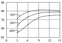
Figure 2 Efficiency (OUTPUT POWER) |
Figure 3 STEP LINE RESPONSE |
 |
 |
|
Figure 4 STEP LOAD RESPONSE |
Figure 5 Start-up overshoot/ delay |
 |
 |
|
Figure 6 Efficiency (OUTPUT POWER) |
Figure 7 STEP LINE RESPONSE |
 |
 |
|
Figure 8 STEP LOAD RESPONSE |
Figure 9 Start-up overshoot/ delay |
 |
|
|
TEMPERATURE (℃) Figure10 Model HHF28S15 |
TEMPERATURE (℃) Figure 11 Model HHF28D15 |
 |
|
|
Figure12 Application Connection Diagram for Single output models |
Figure13 Application Connection Diagram for Dual output models |
 |
 |
|
Figure14 Inhibit Drive connection Diagram for Dual Output Models |
Figure15 Dual Output Converter with EMI Filter Connection Diagram |
 |
|
 |
 |
|
Figure16 Non-flanged outline |
Figure17 Flanged outline |

|
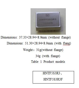
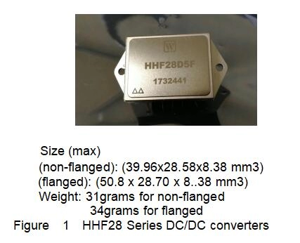
Case Model |
Header |
Header Plating |
Cover |
Cover Plating |
Pin |
Pin Plating |
Sealing Style |
Notes |
|
UPP32727-08f |
Cold Rolled Steel(10#) |
Nickel |
Iron/Nickel Alloy(4J42) |
Nickel |
Copper Compound |
Nickel/Gold |
Compression Seal |
Nickel plating is for pin6. |
 |
 |
|
Figure18 Pin Out Bottom View of non-flanged outline |
Figure19 Pin Out Bottom View of flanged outline |


Subscribe to our weekly newsletter and receive exclusive offers on products you love!
 X
X


 Gold Supplier