| High accuracy |
 |
| Small size | |
| High tracking speed | |
| Uninterrupted tracking during data transfer | |
| Three-state latch output | |
| Low power consumption |
|
Max. absolute rating value |
Supply voltage +VS: 12.5~17.5V |
|
Supply voltage -VS: -17.5~-12.5V |
|
|
Logical voltage VL: 7V |
|
|
Storage temperature range: -40~+100℃ |
|
|
Recommended operating conditions |
Supply voltage +VS: 15V±5% |
|
Supply voltage -VS: -15V±5% |
|
|
Reference voltage (effective value) VRef: nominal value ±10% |
|
|
Signal voltage (effective value) V1*: nominal value ±10% |
|
|
Reference frequency f*: nominal value ±10% |
|
|
Operating temperature range TA: -40~+85℃ |
|
Parameter |
Conditions (-40~+85℃) (Unless otherwise specified) |
(MSDC/MRDC37 series) |
Unit |
|
|
Min. |
Max. |
|||
|
Resolution/RES |
Range of 0~360º |
12 |
16 |
Bit |
|
Tracking speed/St① |
– |
3 |
36 |
rps |
|
High output level/VOH |
TA=25℃ |
2.4 |
– |
V |
|
Low output level/VOL |
TA=25℃ |
– |
0.8 |
V |
|
Power consumption/ PD |
TA=25℃ |
– |
1.3 |
W |
|
Vel linearity/ERl |
TA=25℃ |
– |
1.0 |
% |
|
Range of reference voltage |
– |
2 |
115 |
V |
|
Range of signal voltage |
– |
2 |
90 |
V |
|
Frequency range |
– |
30 |
2 600 |
Hz |
|
Density |
– |
±3 |
±8.5 |
Angular minute |
")


")
|
Pin |
Symbol |
Meaning |
Pin |
Symbol |
Meaning |
Pin |
Symbol |
Meaning |
|
1 |
D1 |
Digital output 1 (highest bit) |
13 |
D13 |
Digital output 13 |
25 |
D16 |
Digital output 16 |
|
2 |
D2 |
Digital output 2 |
14 |
D14 |
Digital output 14 |
26 |
D15 |
Digital output 15 |
|
3 |
D3 |
Digital output 3 |
15 |
RHi |
Reference signal input (high end) |
27 |
Bysel |
Byte select signal |
|
4 |
D4 |
Digital output 4 |
16 |
RLo |
Reference signal input (low end) |
28 |
|
Enable signal |
|
5 |
D5 |
Digital output 5 |
17 |
NC |
Dead end |
29 |
Busy |
Busy signal |
|
6 |
D6 |
Digital output 6 |
18 |
Vel |
Velocity voltage output |
30 |
|
Inhibit signal |
|
7 |
D7 |
Digital output 7 |
19 |
S4 |
Signal input |
31 |
+Vs |
+15V Power supply |
|
8 |
D8 |
Digital output 8 |
20 |
S3 |
Signal input |
32 |
GND |
Power ground |
|
9 |
D9 |
Digital output 9 |
21 |
S2 |
Signal input |
33 |
-Vs |
-15V Power supply |
|
10 |
D10 |
Digital output 10 |
22 |
S1 |
Signal input |
34 |
VL |
+5V Power supply |
|
11 |
D11 |
Digital output 11 |
23 |
R, C |
Zero cross signal |
|
|
|
|
12 |
D12 |
Digital output 12 |
24 |
DIR |
Direction signal |
|
|
|
|
Bit |
Angle |
Bit |
Angle |
Bit |
Angle |
|
1(MSB) |
180,000 0 |
7 |
2,812 5 |
13 |
0,043 9 |
|
2 |
90,000 0 |
8 |
1,406 3 |
14 |
0,022 0 |
|
3 |
45,000 0 |
9 |
0,703 1 |
15 |
0,011 0 |
|
4 |
22,500 0 |
10 |
0,351 6 |
16 |
0,005 5 |
|
5 |
11,250 0 |
11 |
0,175 8 |
|
|
|
6 |
5,625 0 |
12 |
0,087 9 |
|
|
") |
|
|
Fig.10 Connection diagram for typical application of MRDC3756 series |
Fig.11 Interface for direct data reading of MRDC3756 |
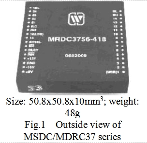
 of Synchro/Resolver-Digital Converter (MSDC/MRDC37 series)")
")


Subscribe to our weekly newsletter and receive exclusive offers on products you love!
 X
X


 Gold Supplier