|
Input DC voltage:28V±1V |
 |
|
Continuous output voltage 10A |
|
|
Peak output current 20A |
|
|
TTL Wide square wave signal input |
|
|
Direction control input signal |
|
|
Isolated between the input signal and output signa |
|
Absolute maximum rating |
Recommended operating conditions |
|
Supply voltage VCC:7V Supply voltage VS:40V Storage temperature:-60~+150℃ Lead welding temperature(10S)Th:300℃ Junction Temperature Tj:150℃ |
Supply voltage VCC:5V±0.25V Supply voltage Vs:28V±1V Operating Temperature(Case):-55~+125℃
|
|
No |
Character |
Conditions (Unless other wise) VCC=5V±0.25V VS=28V±1V -55℃≤Tc≤125℃ RL=10Ω±2Ω |
HISA01-B |
Symbol |
|
|
Min |
Max |
||||
|
1 |
Switching frequency |
Input square wave signal to PWM terminal,DIR direction signal access“0”or“1” |
50 |
- |
HZ |
|
2 |
Continuous output current |
RL=2.4Ωinput high level to PWMterminal,DIR direction signal connect“0”or“1” |
10 |
- |
A |
|
3 |
Peak Drive current |
RL=1.15Ωinput high levelto PWM terminal,DIR direction signal connect“0”or“1” |
20 |
- |
A |
|
4 |
Output square wave voltage amplitude |
Input square wave signal to PWM terminal . DIR=“0”or“1” |
25 |
35 |
V |
|
5 |
Efficiency |
Input high level to PWM terminal , DIR direction signal connect“0”or“1” |
95 |
- |
% |
|
6 |
Static power consumption |
VCC=5V,VS=28V±1V,Full load |
- |
4 |
W |
|
7 |
Disable enable high level |
Input high level to PWM terminal , DIR direction signal connect“0”or“1” |
3.6 |
- |
V |
|
8 |
Disable enable low level |
Input high level to PWM terminal , DIR direction signal connect“0”or“1” |
- |
0.8 |
V |
|
No |
symbol |
Designation |
No |
symbol |
Designation |
|
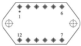
1 |
GND1 |
Input signal Ground |
7 |
SENB |
Load current sensing terminal B |
|
2 |
PWM |
Input PWM signal |
8 |
OUTB |
Output B |
|
3 |
VCC |
+5V power supply |
9 |
VS |
Power Supply |
|
4 |
DIR |
Input direction control signal |
10 |
NC |
NC |
|
5 |
GND |
Output Ground |
11 |
OUTA |
Output A |
|
6 |
NC |
NC |
12 |
SENA |
Load current sensing terminal A |
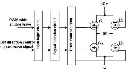

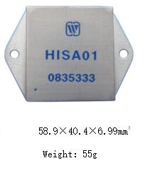
Fig 4 HISA01-B Typical connection Diagram
7.1 Power supply bypass:
Power supply should have sufficient bypass capacitors to ensure proper operation, otherwise it may be unstable and reduce efficiency, and the output may be oscillated. Vs power supply should connect an at least 1uF ceramic capacitor paralleled with a low value ESR capacitor, , the capacitance should be at least 10uF/A ; for VCC also requires a 0.1uF~0.47uF ceramic capacitors paralleled with a low ESR value of 6.8uF~10uF bypass capacitor, All bypass capacitors should be connected as close as possible to the corresponding power supply root.
7.2 The signal input is isolated from the power output
Input PWM ( Pulse Width Modulation) square wave signal ground and DIR direction control signal ground and 5V power supply common ground GNDI connection;Separate form the GNDo of the 28V motor supply to ensure that the signal input is isolated from the power output and that the output is stable and reliable.
7.3 DIR direction control signal input
DIR direction control signal is TTL level signal,Control the direction of the current between the OutA and OutB of the output,thereby controlling the direction of rotation of the motor. The working status of the motor is shown in the form below.
Form 4 working value
|
PWM wide square wave signal(TTL level) |
DIR direction control signal (TTL level) |
OUTA |
OUTB |
DC motor working condition |
|
1 |
0 |
1 |
0 |
Forward |
|
1 |
1 |
0 |
1 |
Reversal |
|
0 |
0 |
0 |
0 |
Stop |
|
0 |
1 |
0 |
0 |
Stop |

|
Symbol |
Data /mm |
||
|
Min |
Typical |
Max |
|
|
A |
6.90 |
- |
7.9 |
|
A1 |
1.9 |
- |
2.7 |
|
Φb |
0.87 |
- |
1.13 |
|
D |
- |
- |
38.80 |
|
E |
- |
- |
41.90 |
|
e |
- |
5.08 |
- |
|
e1 |
- |
30.48 |
- |
|
L |
11.0 |
- |
- |
|
X1 |
49.26 |
- |
50.26 |
|
X |
- |
- |
59.15 |
|
ΦP |
3.70 |
- |
4.30 |

Subscribe to our weekly newsletter and receive exclusive offers on products you love!
 X
X


 Gold Supplier