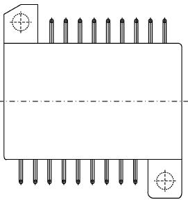
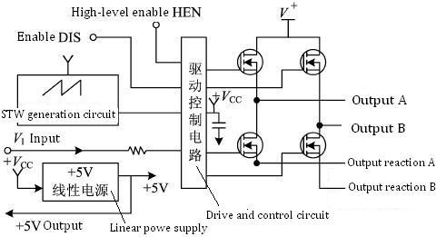
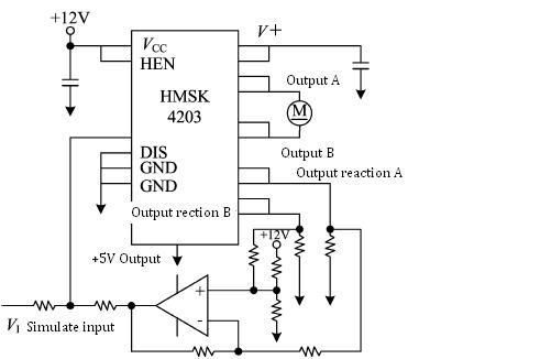
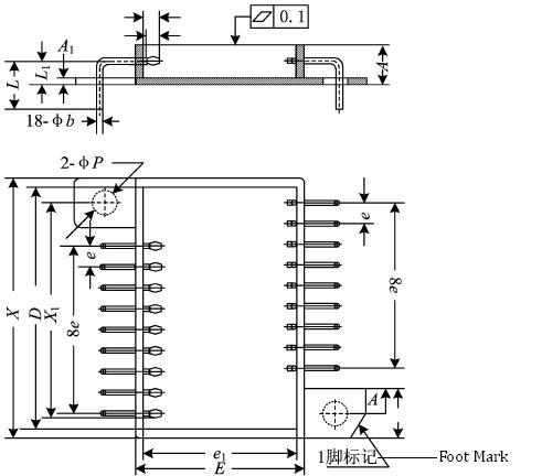
|
+12V single power supply |
 |
|
Widely Input voltage range:16V~75V |
|
|
Continuous output current:10A |
|
|
Peak output current:23A |
|
|
Current-limiting protection function |
|
|
Unipolarity analog signal input, range is 2.5V~9.5V |
|
|
Built-in +5V output |
|
Absolute maximum rated |
Recommended operating conditions |
|
Power supply voltage +VS:75V Output peak current:23A Storage temperature:-65~150℃ Work temperature(TC):-55~125℃ |
Power Supply voltage VCC:12V±0.25V Power Supply voltage VS:16V~48V Working temperature range(Shell temperature):-55~125℃ |
|
No. |
Characteristic |
Test conditions -55℃≤Tc≤125℃ |
HMSK4203 |
Unit |
||||
|
Min |
Typical |
Max |
||||||
|
1 |
On-resistance Rds |
ID=10A |
- |
- |
0.07 |
Ω |
||
|
2 |
MOS Leaky pipeline current |
V+=75V |
- |
- |
150 |
mA |
||
|
3 |
Switching frequency |
- |
40 |
45 |
50 |
KHZ |
||
|
4 |
Continuous working current |
60℃below shell temperature |
- |
10 |
- |
A |
||
|
5 |
Peak working current |
- |
- |
23 |
- |
A |
||
|
6 |
Supply +VS |
- |
16 |
28 |
75 |
V |
||
|
7 |
+VCCStatic current |
IO=0mA |
- |
- |
50 |
mA |
||
|
8 |
+5V Output |
IO=0mA |
4.9 |
5.0 |
5.1 |
V |
||
|
IO=100mA |
4.85 |
5.0 |
5.15 |
V |
||||
|
VI=6V |
40 |
50 |
60 |
% |
||||
|
9 |
Duty cycle of output |
VI=9.5V |
AOUT=100% duty cycle |
|||||
|
BOUT=0% duty cycle |
||||||||
|
VI=2.5V |
AOUT=0% duty cycle |
|||||||
|
BOUT=1000% duty cycle |
||||||||
|
10 |
Enabled output |
VDIS=“0” |
- |
- |
0.8 |
V |
||
|
VDIS=“1” |
2.7 |
- |
- |
V |
||||
|
11 |
High-level enabled output |
VHEN=“0” |
- |
- |
0.8 |
V |
||
|
VHEN=“1” |
2.7 |
- |
- |
V |
||||
|
12 |
Working temperature range(Shell temperature TC) |
- |
-55 |
- |
+125 |
℃ |
||

|
Pin |
Symbol |
Designation |
Pin |
Symbol |
Designation |
|
1 |
VCC |
+12V |
10 |
RSENSE B |
Load current reaction B |
|
2 |
+5V OUT |
+5V Output |
11 |
Output B |
Output B |
|
3 |
DIS |
Enable |
12 |
Output B |
Output B |
|
4 |
HEN |
High-level enable |
13 |
+VS |
Motor supply |
|
5 |
Input |
Signal input |
14 |
+VS |
Motor supply |
|
6 |
NC |
Hang in air |
15 |
Output A |
Output A |
|
7 |
GND |
Ground |
16 |
Output A |
Output A |
|
8 |
GND |
Ground |
17 |
RSENSE A |
Load current reaction A |
|
9 |
RSENSE B |
Load current sense terminal B |
18 |
RSENSE A |
Load current sense terminal A |


|
Symbols |
Data /mm |
||
|
Minimum |
Typical |
Minimum |
|
|
A |
- |
7.4 |
- |
|
A1 |
- |
1.5 |
- |
|
Φb |
0.66 |
0.76 |
0.86 |
|
D |
- |
30.02 |
- |
|
E |
- |
25.40 |
- |
|
e |
- |
2.54 |
- |
|
e1 |
- |
22.40 |
- |
|
L |
8.57 |
8.87 |
9.17 |
|
L1 |
4.2 |
4.45 |
4.70 |
|
X1 |
- |
26.67 |
- |
|
X |
- |
33.02 |
- |
|
ΦP |
- |
3.2 |
- |
 X
X