Synchro to Digital Converters or Resolver to Digital Converters (HSDC/HRDC1746 Series)

Sales Synchro to Digital Converters or Resolver to Digital Converters (HSDC/HRDC1746 Series)

Synchro to Digital Converters or Resolver to Digital Converters (HSDC/HRDC1746 Series) are designed on the principle of type II servo tracking principle and adopts differential isolation input, the data output adopts three-state latch mode, it is suitable for analog signal/digital signal conversion of three-wire synchro and four-wire resolver. With fast conversion speed and stable and reliable performance, this device can be widely applied in angle measurement and automatic control system.
  • Accuracy : ±2 arc min
  • Power supply voltage : +5V,±12V
  • Resolution : 16bits

Product Detail  

1. Features (see Fig. 1 for outside view, and Table 1 for models) of Synchro/Resolver-Digital Converter (HSDC/HRDC1746 Series)

Internal differential isolation conversion

Resolution: 16 bits 
Three-state latch output
Uninterrupted tracking during data transfer 
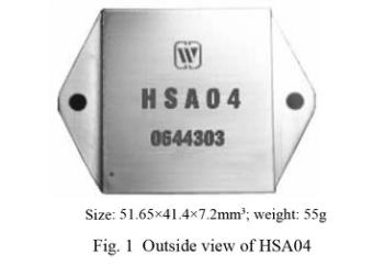
32-wire metal package

2. Scope of application of Synchro to Digital Converters or Resolver to Digital Converters (HSDC/HRDC1746 Series)

Flight instrument system; military servo control system; cannon control system; aviation electronic system; radar control system; naval vessel navigation system; antenna monitoring; robot technology, computerized numeric control (CNC) machine tools; and other automation control system.

3.Description of Synchro to Digital Converters or Resolver to Digital Converters (HSDC/HRDC1746 Series)

HSDC/HRDC1746 series synchro/resolver to digital converter is designed on the principle of type II servo tracking principle and adopts differential isolation input, the data output adopts three-state latch mode, it is suitable for analog signal/digital signal conversion of three-wire synchro and four-wire resolver. With fast conversion speed and stable and reliable performance, this device can be widely applied in angle measurement and automatic control system.
This product is made by the thick-film hybrid integration process and is 32-wire DIP totally sealed metal package. Both the design and manufacture of the product satisfy the requirements of GJB2438A-2002 “General specification for hybrid integrated circuits” and specific specifications of the product.

4. Electrical performance (Table 2, Table 3) of Synchro to Digital Converters or Resolver to Digital Converters (HSDC/HRDC1746 Series)

Table 2  Rated conditions and recommended operating conditions


Table 3  Electricalcharacteristics

Absolute max. rated value

Supply voltage Vs: ± 17.25VDC


Parameter

HSDC/HRDC

1746 Series

Notes

Logical supply voltage VL: +7V


Storage temperature range: -55℃~150℃


Min.

Max.

Recommended operating conditions

Supply voltage Vs: ±15± 5%


Accuracy/angular minute

-2.6

2.6


Effective value of reference voltage VRef: ±10% of nominal value


Tracking speed: rps

-3

3


Effective value of signal voltage V*I:  Nominal value ±5%


Resolution/bit

16


Frequency f*of reference signal: nominal value ±10%


Signal and reference frequency/Hz

50

2.6k


Phase shift between signal and excitation:<±10%


Signal voltage (effective value)/V

2

90


Range of operating temperature (TA):  -40~+105℃


Reference voltage (effective value)/V

2

115


Note: * indicates it can be customized as per user’s requirement.

5. Operating principle of Synchro to Digital Converters or Resolver to Digital Converters (HSDC/HRDC1746 Series)

The synchro input signal (or input signal of resolver) is converted into the orthogonal signal through internal differential isolation:
Synchro/Resolver-Digital Converter (HSDC/HRDC1746 Series)-3
Where, θ is analog input angle
The orthogonal signal is multiplied by the binary digital angle φ in the internal reversible counter in the sine-cosine function multiplier and an error function is obtained:
Synchro/Resolver-Digital Converter (HSDC/HRDC1746 Series)-4
Through error amplification, phase discrimination and filtration of this error function, sin(θ-φ) is obtained, when θ-φ=0 (within the accuracy of the converter), this error will make the voltage controlled oscillator output correction pulse to change the binary digital angle φ of the reversible counter so as to make the output φ value equal to the input θ within the accuracy of the converter, the system becomes stable and can track the change of input angle φ. In this way, a binary digital angle φ representing the input shaft angle θ is obtained on the reversible counter (Fig. 2).
Circuit block diagram
Fig. 2 Circuit block diagram
(1) Dynamic characteristics
Function transfer of the converter
Transfer function of the converter is shown in Fig. 3:
Open-loop gain: Synchro/Resolver-Digital Converter (HSDC/HRDC1746 Series)-6
Closed-loop function:Synchro/Resolver-Digital Converter (HSDC/HRDC1746 Series)-7
For the module of this model Ka=48000/S2, T1=7.1ms, T2=1.25ms Fig. 3  Function transfer of the converter

(2)Methods of data transfer and time sequence
Chip select control Enable

This pin is the input pin of control logic, its function is to output data to the converter to realize three-state control. Low level is valid, the output data of converter occupies the data bus. When it is at high level, the data output pin of converter is in three states, the device does not occupy the bus.
Byte select

This pin is the control input pin, its function is to externally execute selection control on the output data of the converter in the transfer mode of 8-bit data bus or 16-bit data bus. When 16-bit data bus transfer mode is required, keep this logic pin high, the data will be transferred in the bus, the high byte output is in pin D1 to D8 (D1 is high bit) and low byte is in D9 to D16. When 8-bit data bus transfer mode is needed, the data is obtained in pin D1 to D8 (arranged from high to low), and high 8 bits and low 8 bits are obtained through two time sequences, in other words, when Byte select is logic high, high 8 bits are output and when it is logic low, low 8 bits are output.
Data locking control (Inhibit signal ) Inhibit
This pin is the input pin of control logic, its function is to output data externally to the converter to realize optional latching or bypass control. At high level, the output data of the converter is directly output without latching, see the time sequence diagram of the data transfer. At low level, the output data of the converter is latched, the internal loop is not interrupted, and tracking remains working all the time, but the counter doesn’t output data. When it is needed to transfer data, the converter first makes Inhibit control signal to lock the data from high to low, keeps logic low for 640ns, then set Enable input to low (at this time the device occupies the data bus), and then obtains data through Byte select, then turn all control logics to high to refresh and latch the data so as to get ready for transferring the next data, please refer to time sequence diagrams of data transfer Fig.4 and Fig.5.
(3)Attenuation method of input signal (Fig.4 and Fig.5)
 Time sequence of 16-bit bus transfer and Time sequence of 8-bit bus transfer
Fig 4  Time sequence of 16-bit bus transfer                                                 Fig5  Time sequence of 8-bit bus transfer

6. MTBF curve (Fig. 6) of Synchro to Digital Converters or Resolver to Digital Converters (HSDC/HRDC1746 Series)

7. Pin designation (Fig.7, Table 4) of Synchro to Digital Converters or Resolver to Digital Converters (HSDC/HRDC1746 Series)

 MTBF-temperature curve and Pin designation (Bottom view)
Fig.6 MTBF-temperature curve
Fig.7 Pin designation (Bottom view)
(Note: as per GJB/Z299B-98, envisaged good ground condition)

Table 4  Functional description of lead terminals

Pin

Symbol

Meaning

Pin

Symbol

Meaning

1

NC

No connection

17

NC

Leave unconnected

2

D9

Digital output for 9thbit

18

RHi

Input of Resolver RHi

3

D10

Digital output for 10thbit

19

RLo

Input of Resolver RLo

4

D11

Digital output for 11thbit

20

GND

Ground

5

D12

Digital output for 12thbit

21

-VS

-15V power supply

6

D13

Digital output for 13thbit

22

+ VS

+15V power supply

7

D14

Digital output for 14thbit

23

Inhibit

Control of data locking

8

D15

Digital output for 15thbit

24

D1

Digital output for 1st bit

9

D16

Digital output for 16thbit

25

D2

Digital output for 2nd bit

10

Enable

Control of chip select Enable

26

D3

Digital output for 3rd bit

11

Bysel

Byte select

27

D4

Digital output for 4th bit

12

S4NC①

S4input/no connection

28

D5

Digital output 5th bit

13

S3

S3 Input

29

D6

Digital output 6th bit

14

S2

S2 Input

30

D7

Digital output 7th bit

15

S1

S1 Input

31

D7

Digital output 8th bit

16

NC

No connection

32

NC

No connection

Note: ① for HSDC device, S4 is not used.

Table 5  Table of weight values
Table of weight values

8. Connection of the converter of Synchro to Digital Converters or Resolver to Digital Converters (HSDC/HRDC1746 Series)

±15V, +5V and GND shall be connected to corresponding pins on the converter, notice that the polarities of the power supply must be correct, otherwise, the converter may be damaged. It is recommended to connect 0.1μF and 6.8μF bypass capacitance in parallel between each power supply terminal and ground.
Signal and excitation source are allowed to be connected to S1, S2, S3 and S4 and RHi and RLo terminal within an error of 5%.
The signal input shall match the phase of the excitation source so that they can be correctly connected with the converter, their phases are as follows:

For the synchro, signal inputs are:


For the resolver, signal inputs are:


Note: no input signal of RHi, RLo, S1, S2, S3 and S4 is not allowed to be connected to other pins for fear of damage of the device.

9. Package specifications of Synchro to Digital Converters or Resolver to Digital Converters (HSDC/HRDC1746 Series)

Outside view of package
Fig.8 Outside view of package

Table 6  Case materials

Case model

Header

Header plating

Cover

Covering plating

Pinmaterial

Pin plating

Sealing style

Notes

UP4529-32a

Kovar (4J29)

Ni

Iron/ nickel alloy (4J42)

Ni

Kovar (4J29)

Ni/Au

Matchedseal


10. Part numbering key (Fig. 9) of Synchro to Digital Converters or Resolver to Digital Converters (HSDC/HRDC1746 Series)


Part numbering key
Fig.9 Part numbering key of Synchro to digital Converters or Resolver to Digital Converters (HSDC/HRDC1746 Series)

Note: when the above signal voltage and reference voltage (Z) are non-standard, they shall be given as follows:
Synchro/Resolver-Digital Converter (HSDC/HRDC1746 Series)-16
(e.g. reference voltage 5V and signal voltage 3V are expressed as -5/3)
Application notes:
  • Supply the power correctly, upon power-on, be sure to correctly connect the positive and negative pole of the power supply for fear of burning.
  • Upon assembly, the bottom of the product shall fit to the circuit board closely so as to avoid damage of pins, and shockproof provision shall be added, if necessary.
  • Do not bend the pinouts to prevent the insulator from breaking, which affects the sealing property.
  • When the user places an order for the product, detailed electric performance indexes shall refer to the relevant enterprise standard.
Leave A Message
If you are interested in our products and want to know more details,please leave a message here,we will reply you as soon as we can.
X

Home

Supplier

Leave a message

Leave a message

If you are interested in our products and want to know more details,please leave a message here,we will reply you as soon as we can.