|
 |
|
|
|
|
|
|
|
|
|
|
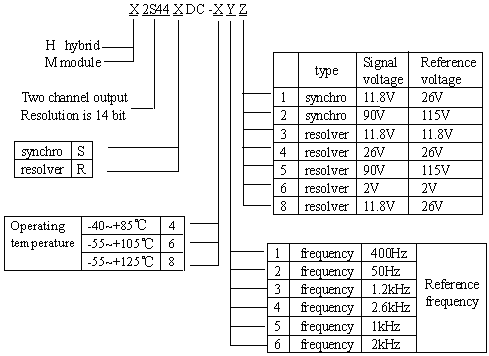
Synchro |
Resolver |
|
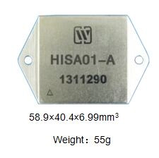
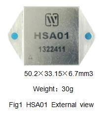
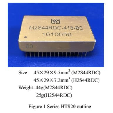
M2S44SDC-61-115/11.8 M2S44SDC-412 H2S44SDC-61-115/11.8 H2S44SDC-412 |
M2S44RDC-418 M2S44RDC-618 M2S44RDC-668 M2S44RDC-658 H2S44RDC-418 H2S44RDC-618 H2S44RDC-668 H2S44RDC-658 |
|
Absolute max nominal value |
power supply voltage Vs:±17V Storage temperature range:-55~+125℃(H2S44) -40~+105℃(M2S44) |
|
Recommended working conditions |
power supply voltage Vs:±15V reference voltage(effective value)Vref:2~115V signal voltage(effective value)VI:2~90V reference frequency f: 50Hz~10kHz operating temperature range TA: -55~+125℃(H2S44) -40~+85℃(M2S44) |
|
Characteristics |
Conditions |
×2S44RDC/SDC Business military standard (Q/HW30826-2006) |
Units |
|||
|
Min |
Max |
|||||
|
Accuracy |
0°~360° |
-5.3 |
5.3 |
Arc min |
||
|
Resolution |
14 |
— |
bit |
|||
|
Output |
VoutHi VoutLo |
2.4 — |
— 0.8 |
V |
||
|
Tracking velocity Repeatability Operating frequency Band width |
20 — 2.6k — |
— 1 50 100 |
Rev/s LSB Hz Hz |
|||
|
input |
VilLo VIHi |
— 2.4 |
0.8 — |
V |
||
|
Gate time of channel tp Time to data stable when A/B state changes Time to data in high impedance when OE is logic “1” power dissipation |
200 — — — |
— 640 200 1.7 |
ns ns ns W |
|||


 ) is the channel select input. Logic “1” selects channel A and Logic “0”
selects channel B. Data become valid 640ns A/ is toggled. Timing
information is shown in fig. 4.
) is the channel select input. Logic “1” selects channel A and Logic “0”
selects channel B. Data become valid 640ns A/ is toggled. Timing
information is shown in fig. 4. )is output enable input. When set to logic “1”,DB1~DB14 are in the high impedance state. When is set to logic “0”,DB1~DB14 represent the angle of transducer
shaft(see bit weights in Table 5) to within the stated accuracy of the
converter. Data become valid 640ns after is switched. Timing information is shown in fig.4.
)is output enable input. When set to logic “1”,DB1~DB14 are in the high impedance state. When is set to logic “0”,DB1~DB14 represent the angle of transducer
shaft(see bit weights in Table 5) to within the stated accuracy of the
converter. Data become valid 640ns after is switched. Timing information is shown in fig.4.
 ) is the built-in test error output. This provides an over velocity and fault indication signal for the channel selected via A/.
The error voltage of each channel is continuously monitored. When the
error exceeds ±50bits for the currently selected channel, is high level, the data are invalid. In normal condition, is low level. is valid for the selected channel approximately 50 ns after the change in the state of A/B. to output high level. It means the converter is in the state of no tracking.
) is the built-in test error output. This provides an over velocity and fault indication signal for the channel selected via A/.
The error voltage of each channel is continuously monitored. When the
error exceeds ±50bits for the currently selected channel, is high level, the data are invalid. In normal condition, is low level. is valid for the selected channel approximately 50 ns after the change in the state of A/B. to output high level. It means the converter is in the state of no tracking.
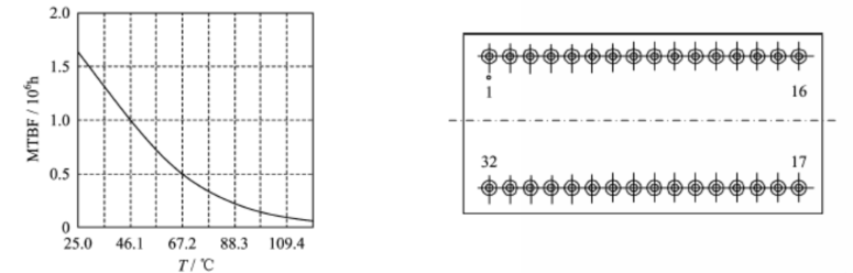
6 MTBF DIAGRAM ( Fig 5 ) of 2S44RDC/SDC Series Two-channel Synchro to Digital converters or Resolver to Digital Converters |
7 PIN CONFIGURATIONS ( Fig6, Tab4 ) of 2S44RDC/SDC Series Two-channel Synchro to Digital converters or Resolver to Digital Converters |
 |
|
|
Figure 5 MTBF vs. temperature Figure 6 Pin out bottom view ( Note: According to GJB/Z 299B-98, assuming that ground is in good condition) |
|
|
Pin |
mnemonic |
description |
Pin |
mnemonic |
description |
|
1~7 8 9 10 11 12 13 14 15 16 |
D8~D14
A/
RLo(A) RHi(A) S4(A) S3(A) S2(A) S1(A) |
Digit output Output enable Channel selection Error detection Channel A reference input high pin Channel A reference input low pin Channel A signal input Channel A signal input Channel A signal input Channel A signal input |
17 18 19 20 21 22 23 24 25 26~32 |
S1(B) S2(B) S3(B) S4(B) RHi(B) RLo(B) GND -Vs +Vs D1~D7 |
Channel B signal input Channel B signal input Channel B signal input Channel B signal input Channel B reference input high pin Channel B reference input low pin Power supply ground -15V power supply +15V power supply Digit output |
|
Bit number |
Weight (degrees) |
Bit number |
Weight (degrees) |
Bit number |
Weight (degrees) |
|
1(MSB) |
180.000 0 |
6 |
5.625 0 |
11 |
0.175 8 |
|
2 |
90.000 0 |
7 |
2.812 5 |
12 |
0.087 9 |
|
3 |
45.000 0 |
8 |
1.406 3 |
13 |
0.043 9 |
|
4 |
22.500 0 |
9 |
0.703 1 |
14 |
0.022 0 |
|
5 |
11.250 0 |
10 |
0.351 6 |
|
|

|
Case model |
Base material |
Base coat |
Lid(cap) material |
Lid(cap) coat |
Lead material |
Lead coat |
Sealing method |
Comments |
|
UP4429-32 |
Kovar (4J29) |
Ni |
Fe/Ni alloy |
Ni |
Kovar (4J29) |
Au |
Match sealing |
|


Subscribe to our weekly newsletter and receive exclusive offers on products you love!
 X
X


 Gold Supplier