|
Absolute Max. Rated value |
|
|
Input voltage:15V~50V Input voltage(Transient,1s):80V Output Power:6.5W Storage temperature:-65℃~150℃ |
Mechanical Shock:1500g Weight(Non-flanged/Flanged):19g/24g The intensity of antistatic:2000V |
|
No. |
Parameter |
Conditions |
HSSA28D5 HSSA28D5F |
HSSA28D12 HSSA28D12F |
HSSA28D15 HSSA28D15F |
||||
|
Q/HW32168-2013 |
Q/HW32169-2013 |
Q/HW32170-2013 |
|||||||
|
Min |
Max |
Min |
Max |
Min |
Max |
||||
|
1 |
Input Voltage/V |
Low、High、Ambient Temperature |
15 |
50 |
15 |
50 |
15 |
50 |
|
|
2 |
Output Voltage/V |
Positive |
Ambient Full load |
4.95 |
5.05 |
11.88 |
12.12 |
14.85 |
15.15 |
|
Negative |
4.95 |
5.05 |
11.88 |
12.12 |
14.85 |
15.15 |
|||
|
Positive |
Low/high Full load |
4.925 |
5.075 |
11.82 |
12.18 |
14.775 |
15.225 |
||
|
Negative |
4.925 |
5.075 |
11.82 |
12.18 |
14.775 |
15.225 |
|||
|
3 |
Output current/A |
VIN=15V~50V |
― |
0.5 |
― |
0.25 |
― |
0.2 |
|
|
4 |
Output Power/W |
|
0 |
5 |
0 |
6 |
0 |
6 |
|
|
5 |
Output Ripple Voltage/mV |
BW≤6MHz,Io=Full load |
― |
50 |
― |
50 |
― |
50 |
|
|
6 |
Line Regulation/mV |
Positive |
VIN=16V~40V,Io=Full |
― |
50 |
― |
50 |
― |
50 |
|
Negative |
― |
50 |
― |
50 |
― |
50 |
|||
|
7 |
Lode Regulation/mV |
Positive |
Io=No load tofull |
― |
50 |
― |
50 |
― |
50 |
|
Negative |
― |
50 |
― |
50 |
― |
50 |
|||
|
8 |
Input current/mA |
Inhibited |
― |
6 |
― |
6 |
― |
6 |
|
|
Io=no load |
― |
60 |
― |
60 |
― |
60 |
|||
|
9 |
Input Ripple current/mA |
BW≤20MHz,Io=Full load |
― |
50 |
― |
50 |
― |
50 |
|
|
10 |
Efficiency/% |
Io=Full load |
66 |
― |
72 |
― |
73 |
― |
|
|
11 |
Isolation/MΩ |
Input to output or any pin to case(except pin 7、8)at 500V,Tc=25℃ |
100 |
― |
100 |
― |
100 |
― |
|
|
12 |
Inhibit Function |
|
0 |
0.7 |
0 |
0.7 |
0 |
0.7 |
|
|
13 |
Under voltage open voltage/V |
Io=Full Load |
12.0 |
14.8 |
12.0 |
14.8 |
12 |
14.8 |
|
|
14 |
Under voltage cut-off voltage/V |
Io=Full Load |
11.0 |
14.5 |
11.0 |
14.5 |
11 |
14.5 |
|
|
15 |
Short Circuit Protection |
|
|
|
|
||||
|
16 |
load/μF |
Tc=25℃ |
― |
500 |
― |
500 |
― |
500 |
|
|
17 |
Io=Full Load |
350 |
500 |
350 |
500 |
350 |
500 |
||
|
18 |
Cross Regulation/mV |
One road 30% load, The other Load 30%→70% |
― |
450 |
― |
450 |
― |
450 |
|
|
19 |
Step Load Response Transient(mV pK) |
50%load→full load or Full load→50% load |
― |
300 |
― |
300 |
― |
300 |
|
|
20 |
Step Load Response Recovery(μs) |
50%load→full load or Full load→50% load |
― |
400 |
― |
450 |
― |
500 |
|
|
21 |
Step Line Response Transient(mV pK) |
VIN:16V→40V, VIN:40V→16V,Io=Full load |
― |
900 |
― |
900 |
― |
900 |
|
|
22 |
Step Line Response Recovery(μs) |
VIN:16V→40V VIN:40V→16V Io=Full load |
― |
700 |
― |
500 |
― |
500 |
|
|
23 |
Start-up Overshoot(mV pK) |
VIN:0→28V, Io=Full load |
― |
25 |
― |
50 |
― |
50 |
|
|
24 |
Start-up Delay (ms) |
VIN:0→28V, Io=Full load |
― |
20 |
― |
20 |
― |
20 |
|


|
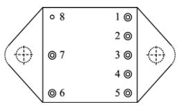
Pin |
Symbol |
Designation |
|
1 |
VO+ |
Positive Output |
|
2 |
GNDO |
Output Common |
|
3 |
VO- |
Negative Output |
|
4 |
NC |
NULL |
|
5 |
INH |
Inhibit |
|
6 |
VIN |
Positive Input |
|
7 |
GNDI |
Input Common |
|
8 |
GNDC |
Case Ground |


 |
 |
|
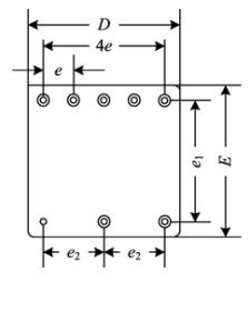
Figure 11 Bottom View |
Figure 12 Side View |
 |
 |
|
Figure 13 Bottom View |
Figure 14 Side View |
|
Dimension Symbols |
Unit/mm |
||
|
Minimum |
Nominal |
Maximum |
|
|
A |
- |
6.86 |
7.16 |
|
Φb |
0.51 |
0.64 |
0.77 |
|
D |
- |
27.23 |
27.57 |
|
E |
- |
27.23 |
27.57 |
|
e |
- |
5.08 |
- |
|
e1 |
- |
20.32 |
- |
|
e2 |
- |
10.16 |
- |
|
L |
4.95 |
5.21 |
- |
|
ΦP |
2.50 |
2.80 |
3.10 |
|
X1 |
- |
39.0 |
39.50 |
|
X2 |
32.90 |
33.20 |
33.50 |
|
Case Model |
Header |
Header Plating |
Cover |
Cover Plating |
Pin |
Pin Plating |
Sealing Style |
Notes |
|
UPP2727-08a (Non-Flanged) |
Cold Rolled Steel(10#) |
Nickel |
Kovar (4J42) |
Nickel |
Copper –coreCompound |
Ni/Au |
Compression Seal |
Nickel Plating is for case ground pin |
|
UPP2727-08u (Flanged) |
Cold Rolled Steel(10#) |
Nickel |
Kovar (4J42) |
Nickel |
Copper –coreCompound |
Ni/Au |
Compression Seal |
Nickel Plating is for case ground pin |


Subscribe to our weekly newsletter and receive exclusive offers on products you love!
 X
X


 Gold Supplier