1.5V  Low Voltage Difference Linear DC to DC converters(LDO)

Sales 1.5V Low Voltage Difference Linear DC to DC converters(LDO)

  • Output Voltage (V) : 1.5V
  • Input DC Voltage (V) : (Vout+1)V

Product Detail  

1 Absolute maximum rated of HSK5176-1.5HTD Series Low Voltage Difference Linear DC to DC converter(LDO)

Pulse input voltageVINP
(Positive pulse width 100ms,positive duty cycle 1%)…-20V~+60V;
Input voltageVIN ……………………………………………………  26V;
Output current limit …………………………………………………7.5A;
Storage temperature Tstg…………………………………… -65℃~150℃;
Lead welding temperature (10s)Th…………………………………300℃;
Junction temperatureTj ……………………………………………175℃;
Thermal resistanceR(th)J-C ………………………………………… 3.5℃/W;
Power consumption PD(Without heat sink)…………………………1W.

2 Recommended operating conditions of HSK5176-1.5HTD Series Low Voltage Difference Linear DC to DC converter(LDO)

Input voltage VIN………………………………………………… (VOUT+1)V;
Operating temperature TC ……………………………………-55℃~125℃.

3 Package Specifications of HSK5176-1.5HTD Series Low Voltage Difference Linear DC to DC converter(LDO)

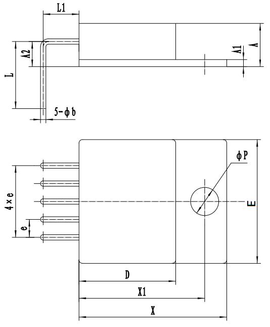
HSK5176-1.5HTD Package outline drawing
Unit:mm

Symbols

Data

Minimum

Typical

Maxim

A

-

-

6.70

A1

0.70

-

1.30

A2

3.20

-

3.80

D

-

-

14.22

E

-

-

18.03

X

-

-

21.30

X1

17.33

-

18.33

L

9.0

-

-

L1

4.58

-

5.58

e

-

2.54

-

φb

0.63

-

0.89

φP

3.70

-

4.30

Fig 19  HSK5176-1.5HTD Package outline drawing

4 Pin Designations of HSK5176-1.5HTD Series Low Voltage Difference Linear DC to DC converter(LDO)

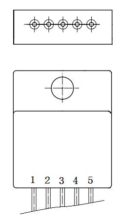
HSK5176-1.5HTD Pin Designations

Pin

Symbol

Designation

1

En

Enable

2

VIN

Input

3

GND

GND

4

VOUT

Output

5

NC

NC

Fig 20  HSK5176-1.5HTD Pin Designations

5  Ordering Information of HSK5176-1.5HTD Series Low Voltage Difference Linear DC to DC converter(LDO)

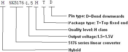
Part number contains the use of the production process, serial number, output voltage, quality level and other information. As shown below:

Ordering Information

6  Technical Specifications of HSK5176-1.5HTD Series Low Voltage Difference Linear DC to DC converter(LDO)

Table 7  HSK5176-1.5 Electrical characteristics

Items

Symbol

Condition (Unless otherwise specified, -55℃≤TA≤125℃)

A Group

Limited value


Unit

Min

Max

Output voltage

VOUT

IOUT =10mA,VIN=2.5V

1,2,3

1.47

1.53

V

Input and output voltage difference

VDO

TA=25℃;△VOUT=-1%;IOUT=250mA

1

800

mV

TA=25℃;△VOUT=-1%;IOUT=7.5A

1200

Static(ground)current

IQ

TA=25℃;VIN=3.5V,IOUT=4A

1

100

mA

TA=25℃;VIN=3.5V,IOUT=7.5A

200

Load regulation

SI

IOUT=10mA→7.0A,VIN=3.0V

1,2,3

2

%

Voltage regulation

SV

VIN=2.5V→26V,IOUT =10mA

1,2,3

1

%

Output noise voltage

VN

TA=25℃;CL=33μF;f≤300KHz

4

700

μV

Output current limit

ILIM

TA=25℃;VIN=2.5V;duty cycle=70%

1

20

A

Thermal shutoff temperature

TSD

TA=25℃;VIN=3.5V;IOUT=5A

4

165


7  Typical Connection Diagram of HSK5176-1.5HTD Series Low Voltage Difference Linear DC to DC converter(LDO)


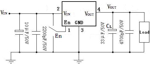
HSK5176-1.5HTD Electrical test line connection diagram
Fig 21  HSK5176-1.5HTD Electrical test line connection diagram

8 Application Notes of HSK5176-1.5HTD Series Low Voltage Difference Linear DC to DC converter(LDO)

☆  The electronic inspecton point should be kept as close as possible at the root of the pin;
☆  It is strictly forbidden to bend the pins;
☆  To prevent the application of two or more absolute maximum ratings on the device at the same time;
☆  To prevent the device from falling off;
☆   To prevent the output and ground short circuit;
☆  To prevent the device from being reversed or dislocated;
☆  During assembly, the bottom of the product should be attached as close as possible to the circuit board to avoid damage to the pin, take shockproof measures for necessary ;
☆  Focus on device power consumption, the power consumption,When the input/output voltage difference(VIN-VOUT) is large, output current IO should be smaller;When the input/output voltage difference(VIN-VOUT)is small ,output current IO should be larger; When the device power consumption is large, be sure to configure the appropriate heat sink to prevent the device damaged due to overheating or into the overheating protection status;
☆  Both positive and negative terminals of power supply shall be correctly connected when power is applied so as to avoid permanent damage to the device.;
☆  Anti-static measures should be taken during storage and transportation.
Leave A Message
If you are interested in our products and want to know more details,please leave a message here,we will reply you as soon as we can.
X

Home

Supplier

Leave a message

Leave a message

If you are interested in our products and want to know more details,please leave a message here,we will reply you as soon as we can.