|
Input DC voltage:30V±2V |
 |
|
Continuous output voltage:10A |
|
|
Peak output current 20A |
|
|
TTL Wide square wave signal input |
|
|
Direction control input signal |
|
|
Isolated between the input signal and output signal |
|
Absolute maximum rating |
Operating conditions |
|
Supply voltage VCC:7V Supply voltage VS:40V Storage temperature:-60~+150℃ Lead welding temperature(10S)Th:300℃ Peak drive current: IOP:10A Junction Temperature Tj:150℃ |
Supply voltage VCC:5V±0.25V Supply voltage Vs:30V±2V Operating Temperature(Case) Tc:-55~+125℃
|
|
No |
Character |
Conditions VCC=5V±0.25V VS=30V±0.3V -55℃≤Tc≤125℃ RL=10Ω±2Ω |
HISA01A |
Symbol |
|
|
min |
max |
||||
|
1 |
Switching frequency |
Input PWM square wave signal,DIR direction signal connect“0”or“1” |
50 |
- |
HZ |
|
2 |
Continuous output current |
Adjusting RL(load resistor) to input PWM square wave signal(The duty cycle is 100% high), DIR direction signal connect“0”or“1” |
3 |
- |
A |
|
3 |
Output square wave voltage amplitude |
Input PWM square wave signal,DIR=0,Output positive unipolar square wave |
26 |
30 |
V |
|
Input PWM square wave signal,DIR=1,Output negative unipolar square wave |
26 |
30 |
V |
||
|
4 |
Efficiency |
Input PWM square wave signal(The duty cycle is 100% high), DIR direction signal connect“0”or“1” |
95 |
- |
% |
|
5 |
Static power consumption |
VCC=5V±0.25V VS=30V±0.3V,Without load RL |
- |
4 |
W |

|
No |
symbol |
Designation |
No |
symbol |
Designation |
|
1 |
GND1 |
Input signal Ground |
7 |
SENB |
Load current sensing terminal B |
|
2 |
PWM |
Input PWM signal |
8 |
OUTB |
Output B |
|
3 |
VCC |
+5V power supply |
9 |
VS |
Power Supply |
|
4 |
DIR |
Input direction control signal |
10 |
NC |
NC |
|
5 |
GND |
Output Ground |
11 |
OUTA |
Output A |
|
6 |
NC |
NC |
12 |
SENA |
Load current sensing terminal A |


|
PWM wide square wave signal(TTL level) |
DIR direction control signal (TTL level) |
OutA |
OutB |
DC motor working condition |
|
1 |
0 |
1 |
0 |
Forward |
|
1 |
1 |
0 |
1 |
Reversal |
|
0 |
0 |
0 |
0 |
Stop |
|
0 |
1 |
0 |
0 |
Stop |
|
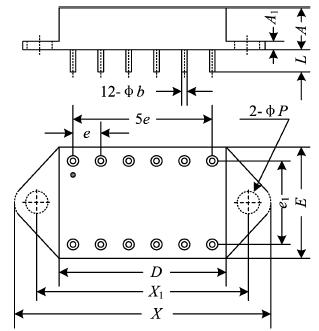
Symbol |
Data /mm |
||
|
Min |
Typical |
Min |
|
|
A |
- |
- |
7.9 |
|
A1 |
1.9 |
- |
2.7 |
|
Φb |
0.87 |
- |
1.13 |
|
D |
- |
- |
38.80 |
|
E |
- |
- |
41.90 |
|
e |
- |
5.08 |
- |
|
e1 |
- |
30.48 |
- |
|
L |
11.0 |
- |
- |
|
X1 |
49.26 |
- |
50.26 |
|
X |
- |
- |
59.15 |
|
ΦP |
3.70 |
- |
4.30 |

Subscribe to our weekly newsletter and receive exclusive offers on products you love!
 X
X


 Gold Supplier