
|
Symbols |
Data |
||
|
Minimum |
Typical |
Maxim |
|
|
A |
10.24 |
- |
10.84 |
|
B |
9.23 |
- |
9.83 |
|
C |
3.4 |
- |
3.8 |
|
D |
3.8 |
- |
4.2 |
|
E |
0.80 |
- |
- |
|
F |
0.70 |
- |
- |
|
H |
- |
- |
3.90 |
|
L |
- |
- |
16.15 |
|
W |
- |
- |
11.71 |

|
Pin |
Symbol |
Designation |
|
1 |
VIN |
Input |
|
2 |
VOUT |
Output |
|
3 |
GND |
GND |

|
Items |
Symbol |
Condition (Unless otherwise specified, -55℃≤TC≤125℃) |
A Group |
Limited value |
Unit |
|
|
Min |
Max |
|||||
|
Output voltage |
VOUT |
IOUT =10mA,VIN=2.5V |
1,2,3 |
1.47 |
1.53 |
V |
|
Input and output voltage difference |
VDO |
TA=25℃;△VOUT=-1%;IOUT=100mA |
1 |
- |
600 |
mV |
|
TA=25℃;△VOUT=-1%;IOUT=3.0A |
- |
700 |
||||
|
Static(ground)current |
IQ |
TA=25℃;VIN=2.5V,IOUT=1.5A |
1 |
- |
40 |
mA |
|
TA=25℃;VIN=2.5V,IOUT=3.0A |
- |
60 |
||||
|
Load regulation |
SI |
IOUT=10mA→2.5A,VIN=2.5V |
1,2,3 |
- |
2 |
% |
|
Voltage regulation |
SV |
VIN=2.5V→26V,IOUT =10mA |
1,2,3 |
- |
1 |
% |
|
Output noise voltage |
VN |
TA=25℃;CL=33μF;f≤300KHz |
4 |
- |
100 |
μV |
|
Output current limit |
ILIM |
TA=25℃;VIN=2.5V |
1 |
- |
5.0 |
A |
|
Thermal shutoff temperature |
TSD |
TA=25℃;VIN=3.5V;IOUT=5.0A |
4 |
- |
160 |
℃ |
|
Items |
Symbol |
Condition (Unless otherwise specified, -55℃≤TC≤125℃) |
A Group |
Limited value |
Unit |
|
|
Min |
Max |
|||||
|
Output voltage |
VOUT |
IOUT =10mA, VIN=2.9V |
1,2,3 |
1.862 |
1.938 |
V |
|
Input and output voltage difference |
VDO |
TA=25℃;△VOUT=-1%;IOUT=100mA |
1 |
- |
500 |
mV |
|
TA=25℃;△VOUT=-1%;IOUT=3.0A |
- |
650 |
||||
|
Static(ground)current |
IQ |
TA=25℃;VIN=2.9V,IOUT=1.5A |
1 |
- |
40 |
mA |
|
TA=25℃;VIN=2.9V,IOUT=3.0A |
- |
60 |
mA |
|||
|
Load regulation |
SI |
IOUT=10mA→2.5A,VIN=2.9V |
1,2,3 |
- |
2 |
% |
|
Voltage regulation |
SV |
VIN=2.9V→26V,IOUT =10mA |
1,2,3 |
- |
1 |
% |
|
Output noise voltage |
VN |
TA=25℃;CL=33μF;f≤300KHz |
4 |
- |
100 |
μV |
|
Output current limit |
ILIM |
TA=25℃;VIN=2.9V |
1 |
- |
5.0 |
A |
|
Thermal shutoff temperature |
TSD |
TA=25℃;VIN=3.9V;IOUT=5.0A |
4 |
- |
160 |
℃ |
|
Items |
Symbol |
Condition (Unless otherwise specified, -55℃≤TC≤125℃) |
A Group |
Limited value |
Unit |
|
|
Min |
Max |
|||||
|
Output voltage |
VOUT |
IOUT =10mA, VIN=3.5V |
1,2,3 |
2.45 |
2.55 |
V |
|
Input and output voltage difference |
VDO |
TA=25℃;△VOUT=-1%;IOUT=100mA |
1 |
- |
150 |
mV |
|
TA=25℃;△VOUT=-1%;IOUT=3.0A |
- |
600 |
||||
|
Static(ground)current |
IQ |
TA=25℃;VIN=3.5V,IOUT=1.5A |
1 |
- |
40 |
mA |
|
TA=25℃;VIN=3.5V,IOUT=3.0A |
- |
60 |
mA |
|||
|
Load regulation |
SI |
IOUT=10mA→2.5A,VIN=3.5V |
1,2,3 |
- |
2 |
% |
|
Voltage regulation |
SV |
VIN=3.5V→26V,IOUT =10mA |
1,2,3 |
- |
1 |
% |
|
Output noise voltage |
VN |
TA=25℃;CL=33μF;f≤300KHz |
4 |
- |
100 |
μV |
|
Output current limit |
ILIM |
TA=25℃;VIN=3.5V |
1 |
- |
5.0 |
A |
|
Thermal shutoff temperature |
TSD |
TA=25℃;VIN=4.5V;IOUT=5.0A |
4 |
- |
160 |
℃ |
|
Items |
Symbol |
Condition (Unless otherwise specified, -55℃≤TC≤125℃) |
A Group |
Limited value |
Unit |
|
|
Min |
Max |
|||||
|
Output voltage |
VOUT |
IOUT =10mA, VIN=4.3V |
1,2,3 |
3.234 |
3.366 |
V |
|
Input and output voltage difference |
VDO |
TA=25℃;△VOUT=-1%;IOUT=100mA |
1 |
- |
150 |
mV |
|
TA=25℃;△VOUT=-1%;IOUT=3.0A |
- |
600 |
||||
|
Static(ground)current |
IQ |
TA=25℃;VIN=4.3V,IOUT=1.5A |
1 |
- |
40 |
mA |
|
TA=25℃;VIN=4.3V,IOUT=3.0A |
- |
60 |
mA |
|||
|
Load regulation |
SI |
IOUT=10mA→2.5A,VIN=4.3V |
1,2,3 |
- |
2 |
% |
|
Voltage regulation |
SV |
VIN=4.3V→26V,IOUT =10mA |
1,2,3 |
- |
1 |
% |
|
Output noise voltage |
VN |
TA=25℃;CL=33μF;f≤300KHz |
4 |
- |
150 |
μV |
|
Output current limit |
ILIM |
TA=25℃;VIN=4.3V |
1 |
- |
5.0 |
A |
|
Thermal shutoff temperature |
TSD |
TA=25℃;VIN=5.3V;IOUT=5.0A |
4 |
- |
160 |
℃ |
|
Items |
Symbol |
Condition (Unless otherwise specified, -55℃≤TC≤125℃) |
A Group |
Limited value |
Unit |
|
|
Min |
Max |
|||||
|
Output voltage |
VOUT |
IOUT =10mA, VIN=6.0V |
1,2,3 |
4.90 |
5.10 |
V |
|
Input and output voltage difference |
VDO |
TA=25℃;△VOUT=-1%;IOUT=100mA |
1 |
- |
150 |
mV |
|
TA=25℃;△VOUT=-1%;IOUT=3.0A |
- |
600 |
||||
|
Static(ground)current |
IQ |
TA=25℃;VIN=6.0V,IOUT=1.5A |
1 |
- |
40 |
mA |
|
TA=25℃;VIN=6.0V,IOUT=3.0A |
- |
60 |
mA |
|||
|
Load regulation |
SI |
IOUT=10mA→2.5A,VIN=6.0V |
1,2,3 |
- |
2 |
% |
|
Voltage regulation |
SV |
VIN=6.0V→26V,IOUT =10mA |
1,2,3 |
- |
1 |
% |
|
Output noise voltage |
VN |
TA=25℃;CL=33μF;f≤300kHz |
4 |
- |
300 |
μV |
|
Output current limit |
ILIM |
TA=25℃;VIN=6.0V |
1 |
- |
5.0 |
A |
|
Thermal shutoff temperature |
TSD |
TA=25℃;VIN=7.0V;IOUT=5.0A |
4 |
- |
160 |
℃ |

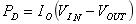 ,When the input/output voltage difference(VIN-VOUT) is large, output current IO should be smaller;When the input/output voltage difference(VIN-VOUT)is small ,output current IO should be larger; When the device power consumption is large, be sure to configure the appropriate heat sink to prevent the device damaged due to overheating or into the overheating protection status;
Subscribe to our weekly newsletter and receive exclusive offers on products you love!
 X
X


 Gold Supplier