HSA03-C High Power Pulse Width Modulation Amplifiers

Sales HSA03-C High Power Pulse Width Modulation Amplifiers

  • Max.Input Vol : 100V
  • Function : BRUSHED DC MOTOR CONTROLLER
  • Max Current : 30A

Product Detail  

1.  Features

Widely motor input voltage range :16V~100V

TTL square wave signal input
Maximum Continuous output current : 30A
Overheat Current-limiting protection function

2. Scope of application of HSA03-C High Power Pulse Width Modulation Amplifier

Motor controlling with brush
Drive reactive load

3.  Descriptions of HSA03-C High Power Pulse Width Modulation Amplifier

HSA03-C is a pulse width modulation type power amplifier which operates in the switching mode, it can provide 3KW maximum transmission power for the load; the product needs two power supplies, + 15v for the small signal control circuit power supply; 16v-100v motor the power supply for the internal H bridge. The input signal of the input circuit is 50KH TTL TTL signal; the key input can turn off the four drive tubes of the H bridge circuit.
The series of the products are made of thick film hybrid integrated process, metal sealed shell package. Product design and manufacturing to meet the MIL-STD and detailed specifications of the product requirements, the quality level is H-class.

4. Technical Specifications of HSA03-C High Power Pulse Width Modulation Amplifier

Table 1: Rated conditions and Recommended operating conditions

Absolute maximum rating

Recommended operatingconditions

Supply voltage +Vs:100V

Supply voltage +Vcc:16V

Input voltage +PWM:0V~11V

Input voltage -PWM:0V~11V

Input voltage,Ilimit/SHDN:0~+10V

Internal power loss:380W

Storage temperature(10s):-65℃~150℃

Operating temperature:-55℃~125℃

Supply voltage +Vcc:15V

Supply voltage +Vs:100V

Input voltage +PWM:+3V~+7V

Input voltage,Ilimi/SHDN:≥0.1V


Table 2 electrical characteristics


No.

Character

Conditions

-55℃≤Tc≤125℃

HSA03-C

Symbol

min

Typical value

max

1

Outputclock high level

-

4.8

-

5.3

V

2

Outputclock lowlevel

-

0

-

0.4

V

3

clockoutputfrequency

-

42

45

48

KHZ

4

triangularwavecenter voltage

-

-

5

-

V

5

triangular wave peak

-peak voltage

-

-

4

-

V

6

switchingoperation frequency

-

-

22.5

-

KHZ

7

outputefficiency

VS=100V,output current10A

-

97

-

%

8

Continuous working current

Below60℃(case temperature)

-

-

30

A

9

Peak working current

-

-

-

40

A

10

Power +Vs

-

16

-

100

V

11

Power +Vcc

-

14

15

16

V

12

+Vccstatic current

Iout=0

-

-

80

mA

13

+Vspower current

No load

-

-

50

mA

14

Ilimit/shutoff  threshold

-

3.9

-

-

mV

15

Operating Temperature(shell temperature)

-

-55

-

+125


5. Lead function descriptions of HSA03-C High Power Pulse Width Modulation Amplifier

Lead function descriptions

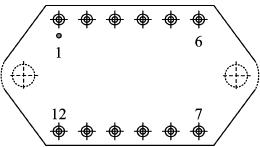
Fig  2 upward view

Table 3  Pin Designation

No

symbol

Designation

No

symbol

Designation

1

CLK IN

Clockinput

7

ISENSEB

Load current inductor B


2

CLK Out

Clock output

8

Bout

Output B

3

+PWM

TTL PWM square wave

9

+Vs

motor power

4

VRef

2.5V

10

+Vcc

+15V power

5

GND

Ground

11

A out

output A

6

I limit/SHDN

Currentlimiter/

shut off

12

ISenseA

Load current inductor A


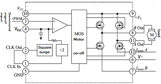
6. Circuit block diagram of HSA03-C High Power Pulse Width Modulation Amplifier

Circuit block diagram
Fig 3  Circuit block diagram

7. Typical Connection Diagram of HSA03-C High Power Pulse Width Modulation Amplifier

HSA03-C Power supply has two current sampling end ISENSEA and ISENSEB.The two terminals shall be shorted when using voltage control model . The typical connection diagram as shown in Fig 4.

Typical Connection Diagram
7.1 Power supply bypass
HSA03-C power supply should have plenty of bypass to ensure its correct operation, the motor power supply should add a ceramic capacitor C3, and then in parallel with a low ESR value of the bypass capacitor C4, the capacitance should be at least 10uf / A .for VCC the same , a 0.1 μF-0.47μF / 50V ceramic capacitor C1 and a low ESR value of 6.8μF-10μF/50V bypass capacitor C2. All bypass capacitors should be connected as close as possible to the corresponding root of  power port.

7.2  Unprotected circuit typical connection diagram
If the system does not need current limiting protection circuit, you can connect as in Figure 5


Fig  5  unprotected circuit typical connection diagram

8. Package Specifications of HSA03-C High Power Pulse Width Modulation Amplifier


Package Specifications
Fig6 package outline drawing

Form 4  Package Outline

Symbol

Data/mm


Min

Typical

Min

A

-

-

6.99

A1

2.28

-

2.44

Φb

1.47

-

1.57

D

-

-

40.40

E

-

-

40.40

e

-

5.08

-

e1

-

30.48

-

L

11.43

-

12.70

X1

49.56

-

49.96

X

-

-

58.90

ΦP

3.80

-

4.20


Application notes please refer to the appendix, must read it carefully.
Leave A Message
If you are interested in our products and want to know more details,please leave a message here,we will reply you as soon as we can.
X

Home

Supplier

Leave a message

Leave a message

If you are interested in our products and want to know more details,please leave a message here,we will reply you as soon as we can.