MDSC/MDRC28 Series Digital to Synchro Converters or Digital to Resolver Converters

Sales MDSC/MDRC28 Series Digital to Synchro Converters or Digital to Resolver Converters

MDSC/MDRC28 Series Digital to Synchro Converters or Digital to Resolver Converters are that converts the input binary signal to that of synchro or resolver. The input signal is compatible with DTL/TTL/CMOS level, and the output is 3-wire synchro or 4-wire resolver signal. This series of product continuously tracks the input 12-bit/14-bit/16-bit binary data, and outputs high-precision synchro/resolver signal after conversion. The product is equipped with power amplification circuit inside it, and its output power can reach 1.5W.
  • Accuracy : ±8 arc min(12 bits), ±4 arc min(14 bits), ±4 arc min(16 bits)
  • Resolution : 12, 14 or 16 bits
  • Power supply voltage : ±15V

Product Detail  

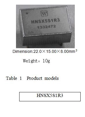
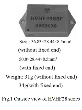
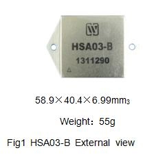
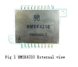
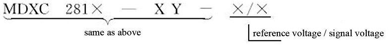
1.Features (see Fig. 1 for outside view, and Table 1 formodels)

Compatible with DTL/TTL/CMOS level

12-bit, 14-bit and 16-bit resolution
Short-circuit and overload protection
Metal case, with good heatsinking
Output power: 1.5W


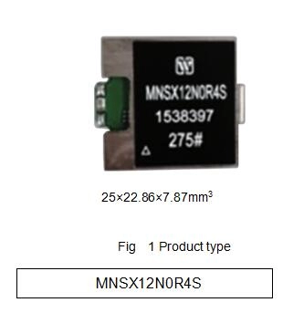
Table1 Product models

12-bit

14-bit

16-bit

Synchro

Resolver

Synchro

Resolver

Synchro

Resolver

MDSC2812-411

MDRC2812-418

MDSC2814-411

MDRC2814-418

MDSC2816-411

MDRC2816-418

MDSC2812-412

MDRC2812-438

MDSC2814-412

MDRC2814-438

MDSC2816-412

MDRC2816-438

MDSC2812-421

MDRC2812-414

MDSC2814-421

MDRC2814-414


MDRC2816-414

MDSC2812-422

MDRC2812-415

MDSC2814-422

MDRC2814-415


MDRC2816-41-36/11.8


MDRC2816-415


2. Scope of application of MDSC/MDRC28 Series Digital to Synchro Converters or Digital to Resolver Converters

Military servo-control system; antenna system; radar measurement system; navigation system; cannon control system; machine-tool control.


3. Description of MDSC/MDRC28 Series Digital to Synchro Converters or Digital to Resolver Converters

MDSC/MDRC28 series product is a converter that converts the input binary signal to that of synchro or resolver. The input signal is compatible with DTL/TTL/CMOS level, and the output is 3-wire synchro or 4-wire resolver signal. This series of product continuously tracks the input 12-bit/14-bit/16-bit binary data, and outputs high-precision synchro/resolver signal after conversion. The product is equipped with power amplification circuit inside it, and its output power can reach 1.5W.

4. Electrical performance (Table 2, Table 3) of MDSC/MDRC28 Series Digital to Synchro Converters or Digital to Resolver Converters

Table 2  Rated conditions and recommended operating conditions

Absolute max. rated value

Supply voltage +VS: +13.5~+17.5V

Supply voltage -VS: -17.5~-13.5V

Storage temperature range: -40~100℃

Recommended operating conditions

Supply voltage +VS: +14.5~+16.5V

Supply voltage -VS: -16.5~-14.25V

Reference voltage (effective value) VRef: 115V±5%

Signal voltage (effective value) V1: 90V±5%

Reference frequency f: 400Hz±10%

Range of operating temperature TA: -40℃~85℃

Note: * indicates it can be customized as per user’s requirement.

Table 3  Electric characteristics

Parameter

MDRC/MDSC2812

MDRC/MDSC2814

Enterprise military standard (Q/HW30857-2006)

MDRC/MDSC2816

Resolution

Accuracy

Digital input

Reference voltage (effective value)

Reference frequency

12-bit

±8

12-bit binary code

14-bit

±4

14-bit binary code

26V/115V/4V

50Hz/400Hz

16-bit

±4

16-bit binary code

Output signal voltage

(Effective value)

11.8V (line-line, resolver or synchro)

90V (line-line, resolver or synchro)

Input data speed

Step response time

Output power


Note: * means the products with different frequency and different amplitude can be made according to the user’s need.

5. Operating principle (Fig. 2 and Fig. 3) of MDSC/MDRC28 Series Digital to Synchro Converters or Digital to Resolver Converters

One of the distinctive characteristics of MDSC/MDRC28 series product is that it can neglect the change of radius vector. Each type of digital converter to syncrho/resolver must be provided with output sin and cos function signal, however, since the law of sin and cos function is not followed precisely all the time, its error can reach ± 7%. In practical use, this error is not serious sometimes, but it is not allowed in the application of tracking rotating torque receiver or servo control loop. For MDSC/MDRC28 series product, this error can be reduced below 0.1%, which means that when the converter is used in a closed loop servo system, the closed-loop gain is independent of the input signal, thus avoiding undesired error resulting from change of reference signal.


Fig.2  Schematic diagram of MDSC converter
Fig.2  Schematic diagram of MDRC converter

6. MTBF curve (Fig. 4) of MDSC/MDRC28 Series Digital to Synchro Converters or Digital to Resolver Converters

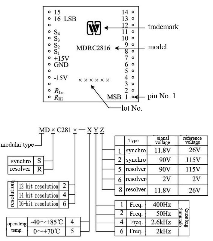
7. Pin designation (Fig. 4, Table 4) of MDSC/MDRC28 Series Digital to Synchro Converters or Digital to Resolver Converters


Fig. 4  MTBF-temperature curve
(Note: according to GJB/Z299B-98, envisaged good ground condition)

Fig.5  Schematic diagram of pins


Table 4  Pin designation

Pin

Symbol

Function

Pin

Symbol

Function

Pin

Symbol

Function

1

1 (MSB)

Digital input 1

11

11

Digital input 11

21

S1

Signal output 1

2

2

Digital input 2

12

12

Digital input 12

22

+15V

+15V input

3

3

Digital input 3

13

13

Digital input 13

23

GND

Ground

4

4

Digital input 4

14

14

Digital input 14

24

NC

Leave unconnected

5

5

Digital input 5

15

15

Digital input 15

(12-bit and 14-bit are leave unconnected)

25

-15V

-15V input

6

6

Digital input 6

16

16

Digital input 16

(12-bit and 14-bit are leave unconnected)

26

NC

Leave unconnected

7

7

Digital input 7

17

NC

Leave unconnected

27

RLo

Low end of reference input

8

8

Digital input 8

18

S4

Signal output 4

28

RHi

High end of reference input

9

9

Digital input 9

19

S3

Signal output 3


10

10

Digital input 10

20

S2

Signal output 2


Notes:
① Digital input: DSC/DRC292 is 1~12, altogether 12 bits; DSC/DRC2914 is 1~14, altogether 14 bits; DSC/DRC2916 is 1~16, altogether 16 bits.
② “1” is the highest bit (MSB);
③ S1, S2, S3 and S4:output are used for synchro or resolver, among them, S4 is only used for resolver;
④ RHi and RLo: reference input;
⑤GND: common ground of power supply and input signal;
⑥±15V: power supply.

8. Table of weight values (Table 5) of MDSC/MDRC28 Series Digital to Synchro Converters or Digital to Resolver Converters

Table 5  Table of weight values

Bit (MSB)

Angle

Bit (MSB)

Angle

Bit (MSB)

Angle

1

180.000 0

6

5.625 0

11

0.175 8

2

90.000 0

7

2.812 5

12 (for 12-bit LSB)

0.087 9

3

45.000 0

8

1.406 3

13

0.043 9

4

22.500 0

9

0.703 1

14 (for 14-bit LSB)

0.022 0

5

11.250 0

10

0.351 6


9. Connection diagram for typical application (Fig. 6) of MDSC/MDRC28 Series Digital to Synchro Converters or Digital to Resolver Converters

DSC/DRC load connection
(1)Control transformer (CT)
The simplest design is using digital converter to synchro/resolver to drive the control transformer. The min. power for driving CT is:

Where, V is line-line voltage, Zso is the impedance between nodes after the circuit from one output end of CT to other two rotor circuits is short-circuited (Zso=Rso+jXso).
For example: when the impedance of CT is ZS=700+j490, the line-line voltage is 90V, then

For the adjustment of CT load, it can be reduced through 3 capacitances at the output end, as shown as below:


Fig. 6 Connection diagram for typical application

The required power is: (VA) (unadjusted) x
In the above example, the capacitance is:
The required power after adjustment is:
In the design, it is required to note the errors that usually exist such as coil number, capacitance, inductance, etc. in CT.

Practical prompts for CT load adjustment:
① High precision capacitance is not required, an error of 20% is enough.
② Three capacitances must be used between S1 and S2, S2 and S3 as well as S3 and S1.
③ Withstand voltage and type of capacitance
For line-line voltage of 11.8V, the withstand voltage of capacitance between pins is 25VAC, and the type of capacitance is non-polar tantalum capacitance.
For line-line voltage of 90V, the withstand voltage of capacitance between pins is 150VAC, and it is allowed to use ceramic capacitance with low dielectric constant.
④ The load adjustment of resolver only requires two capacitances. One is connected between S1 and S3, and the other between S2 and S4.
(2)Control differential transducer (CDX)
The load of DSC in the equipment can be considered like CT load, but its equivalent impedance Z must be calculated like CT load, its value is generally 66%~80% of ZSO.
(3)Torque receiver (TR)
Compared with CT and CDX, it is relatively difficult to control the torque receiver (TR). Generally speaking, it requires an output amplifier. Because the change of radius vector of MDSC/MDRC28 series product can be neglected, it is more suitable for controlling TR than those devices with an error of ±7%. For an error with angle θ, the exciting current is:

Prompts:
① TR should not be blocked.
② The corresponding advance from reference input end to DSC shall conform to the provisions of TR.
③ The reference input must be always applied on TR and converter.
④ The output voltage of DSC/DRC must completely match with the voltage required by TR.

10. Package specifications (unit: mm) (Fig. 7) of MDSC/MDRC28 Series Digital to Synchro Converters or Digital to Resolver Converters


Fig. 7 Outside view and dimensions of package

11. Part numbering key (Fig. 8) of MDSC/MDRC28 Series Digital to Synchro Converters or Digital to Resolver Converters


Fig. 8 Part numbering key

Note: when the above signal voltage and reference voltage (Z) are non-standard, they shall be given as follows:


(e.g. reference voltage 40V and signal voltage 38V are expressed as -40/38)


Application notes


  • Do not apply reference voltage of 115V to the device of 26V.
  • The voltage of power supply shall not exceed the specified range.
  • Do not connect reference RHi and RLo to other pins.
  • Supply voltage must be kept to the voltage of correct polarity.
  • When the max. absolute rated value is exceeded, the device may be damaged.
  • Upon assembly, the bottom of the product shall fit to the circuit board closely so as to avoid damage of pins, and shockproof provision shall be added, if necessary.
  • When the user places an order for the product, detailed electric performance indexes shall refer to the relevant enterprise standard.
Leave A Message
If you are interested in our products and want to know more details,please leave a message here,we will reply you as soon as we can.
X

Home

Supplier

Leave a message

Leave a message

If you are interested in our products and want to know more details,please leave a message here,we will reply you as soon as we can.