HSA03-A High Power Pulse Width Modulation Amplifiers

Sales HSA03-A High Power Pulse Width Modulation Amplifiers

  • Max.Input Vol : 100V
  • Max Current : 30A
  • Function : BRUSHED DC MOTOR CONTROLLER

Product Detail  

1. Features

Compatible with APEX SA03 and MSK MSK4205

Widely motor input voltage range:16V~100V
Analog signal circuit input
Max Continuous output current : 30A
Overheat Current-limiting protection function

2. Scope of application of HSA03-A High Power Pulse Width Modulation Amplifier

Motor controlling with brush
Drive reactive load

3. Descriptions of HSA03-A High Power Pulse Width Modulation Amplifier

HSA03-A is a pulse width modulation type power amplifier which operates in the switching mode, it can provide 3KW maximum transmission power for the load; the product needs two power supplies, + 15v for the small signal control circuit power supply; 16v-100v motor The power supply for the internal H bridge. The control signal of the input circuit is the DC level signal of 3v-7v. The internal output 45KHZ TTL wave signal, the output width of the square wave signal frequency is 22.5KHZ. The key input can turn off the four drive tubes of the H-bridge circuit.
The series of the products are made of thick film hybrid integrated process, metal sealed shell package. Product design and manufacturing to meet the MIL-STD and detailed specifications of the product requirements, the quality level is H-class.

4. Technical Specifications of HSA03-A High Power Pulse Width Modulation Amplifier

Table 1 Rated conditions and Recommended operating conditions

Absolute maximum rating

Recommended operating conditions

Supply voltage +Vs:100V

Supply voltage +Vcc:16V

Input voltage  +PWM:0~+11V

Input voltage -PWM:0~+11V

Input voltage,Ilimit/SHDN:0~+10V

Internal power loss:380W

Storage temperature(10s):-65℃~150℃

Operating Temperature(Tc):-55℃~125℃

Supply voltage +Vs:100V

Supply voltage +Vcc:15V

Input voltage +PWM:+3V~+7V

Input voltage Ilimit/SHDN:0.1V


Table 2 electrical characteristics

No

Character

Conditions

-55℃≤Tc≤125℃
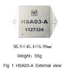
HSA03-A

Symbol

min

Typical value

max

1

Output clock high level

-

4.8

-

5.3

V

2

Output clock low level

-

0

-

0.4

V

3

clock output frequency

-

42

45

48

KHZ

4

triangular center voltage

-

-

5

-

V

5

triangular wave peak

-peak voltage

-

-

4

-

V

6

Switching  operation frequency

-

-

22.5

-

KHZ

7

output efficiency

VS=100V,output current 10A

-

97

-

%

8

Continuous working current

Below60℃

-

-

30

A

9

Peak working current

-

-

-

40

A

10

Power+Vs

-

16

-

100

V

11

Power+VCC

-

14

15

16

V

12

+VCCstatic current

Io=0

-

-

80

mA

13

+Vspower current

No load

-

-

50

mA

14

Ilimit/Shutoff  threshold

-

90

-

110

mV

15

Operating Temperature(shell temperature)

-

-55

-

+125


5. Lead function descriptions of HSA03-A High Power Pulse Width Modulation Amplifier

Lead function descriptions
Fig  2 upward view

Table 3  Pin Designation

No

symbol

Designation

No

symbol

Designation

1

CLK IN

Clockinput

7

Isense B

Load currentsensing terminal B


2

CLK Out

Clockoutput

8

Bout

Output B

3

+PWM

+PWM input signal

9

+VS

motor power

4

-PWM/RAMP

-PWM input signal/

or internaltriangular wave output

triangular output

10

+VCC

+15V power

5

GND

Ground

11

Aout

output A

6

Ilimit/SHDN

current limiter/

shut off

12

Isense A

Load currentsensing terminal A


6. Circuit block diagram of HSA03-A High Power Pulse Width Modulation Amplifier

Circuit block diagram
Fig  3  Circuit block diagram

7. Typical Connection Diagram of HSA03-A High Power Pulse Width Modulation Amplifier

HSA03-A power supply should have plenty of bypass to ensure its correct operation, the motor power supply should add a ceramic capacitor C3, and then in parallel with a low ESR value of the bypass capacitor C4, the capacitance should be at least 10uf / A .for VCC the same , a 0.1 μF-0.47μF / 50V ceramic capacitor C1 and a low ESR value of 6.8μF-10μF/50V bypass capacitor C2. All bypass capacitors should be connected as close as possible to the corresponding root of  power port.

Typical Connection Diagram

Fig 4  HSA03-A Typical connection diagram
Power supply bypass
Power supply should have plenty of bypass to ensure its correct operation, the motor power supply VS should add a 1μF ceramic capacitor, and then in parallel with a low ESR value of the bypass capacitor, the capacitance should be at least 10uF/ A .for VCC the same , a 0.1 μF-0.47μF ceramic capacitor and a low ESR value of 6.8μF-10μF bypass capacitor. All bypass capacitors should be connected as close as possible to the corresponding root of power port.

8. Package Specifications of HSA03-A High Power Pulse Width Modulation Amplifier

Package Specifications
Fig5 package outline drawing

Form 4  Package Outline

Symbol

Data/mm


Min

Typical

Min

A

-

-

6.99

A1

2.28

-

2.44

Φb

1.47

-

1.57

D

-

-

40.40

E

-

-

40.40

e

-

5.08

-

e1

-

30.48

-

L

11.43

-

12.70

X1

49.56

-

49.96

X

-

-

58.90

ΦP

3.80

-

4.20

Application notes please refer to the appendix, must read it carefully
Leave A Message
If you are interested in our products and want to know more details,please leave a message here,we will reply you as soon as we can.
X

Home

Supplier

Leave a message

Leave a message

If you are interested in our products and want to know more details,please leave a message here,we will reply you as soon as we can.