5.2W Non-isolated Point of Load DC to DC Converters (POL)

Sales 5.2W Non-isolated Point of Load DC to DC Converters (POL)

  • Output Voltage (V) : 1V
  • Input DC Voltage (V) : 4.5V-5.5V
  • Max. Output Power (W) : 5.2W

Product Detail  

1 Features of HNSX5S Series Non-isolated Point of Load DC/DC Converters (POL)

High reliability
Width input voltage range:4.5V~5.5V,Nominal
DC input voltage: 5V
High Conversion Efficiency
Output Power PO:5.2W
Operating temperature range Tc:-55℃~+125℃
Low Startup current
No output overshoot
Inhibit function
output short circuit protection
Maximum power density:34W/in3
Hermetically sealed metal case


2. Scope of application of HNSX5S Series Non-isolated Point of Load DC to DC Converters (POL)

High-reliability electronic system for ground, vehicle, radar, aviation and aerospace, etc

3. Descriptions of HNSX5S Series Non-isolated Point of Load DC to DC Converters (POL)
This device is a high-reliability, output voltage trimmable non-isolated DC DC Converters. Buck circuit topology and the principle of pulse width modulation are used in devices. The output voltage will regulate the pulse width of the controller by direct sampling feedback to ensure the stable output voltage. Output voltage can be 0.9V~1.3V  adjustable by the variation of externally connected resistor .The series of devices use thick-film hybrid integrated process and metal sealed enclosure package. The design and manufacturing process of HNSX5S Series converters are in compliance with MIL-PRF-38534 and detailed specifications

4. Technical Specifications of HNSX5S Series Non-isolated Point of Load DC to DC Converters (POL)

Table  2  Rated conditions and recommended operating conditions

Absolute Max. Rating

Input voltage:4.5V~5.5V

Input voltage(Transient,1s):6V

Output Power:5.5W

Storage temperature:-65℃~150℃

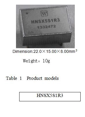
Mechanical Shock:1500g

Lead resistance welding temperature:300℃(15s)

Weight:10g

ESD>2000V


Table 3 Electrical characteristics

No.

Items

Conditions (Testing condition as per-55℃≤TC≤125℃,VIN=5V±0.5, unless otherwise specified)

HNSX5S1R3

Min

Max

1

Input Voltage/V

Low、High、Ambient Temperature

4.5

5.5

2

Output Voltage/V

Io=Full Load

Ambient、Low、high Temperature

0.86

0.94

0.96

1.04

1.25

1.35

3

Output current/A

VIN=4.5V~5.5V

4

4

Output Power/W


0

5.2

5

Output Ripple Voltage/mV

Vo=1.0V,IO=4A,BW=20MHz

30

6

Line Regulation/mV

VIN=4.5V~5.5V,Vo=1.0V,IO=4A

30

7

LoadRegulation/mV

Vo=1.0V,IO=0→4A

30

8

Efficiency/%

Vo=1.0V,IO=4A

70

9

Isolation/MΩ

TA=25℃,any pin to case at 500V DC

500

10

Inhibitvoltageswitch-off voltage/V

Vo=1.0V,IO=4A

0

0.8

11

Inhibit voltage open voltage/V

Vo=1.0V,IO=4A

2.4

-

12

Inhibit Current/mA

TA=25℃,Vo=1.0V,IO=4A,Inhibit pin to ground

-

10

13

Protection/s

TA=25℃,Vo=1.0V

-

2

14

Under voltage open voltage/V

TA=25℃,Vo=1.0V,IO=4A

2.4

4.3

15

Under voltageswitch-off voltage/V

TA=25℃,Vo=1.0V,IO=4A

2.2

3.7

16

Voltagetolerance of the set point/V

-55℃≤TC≤85℃,Vo=1.0V,IO=3A

0.96

1.04

17

Inputtransient Voltage/V

Vo=1.0V,IO=4A

-

6

18

Capacitive load/μF

Vo=1.0V,IO=4A,No effect for DC

1000

19

switching frequency/kHz

Vo=1.0V,IO=4A

600

750

20

Step Load Response Transient(mV pK)

Vo=1.0V,IO=2A→4A orIO=4A→2A

300

21

Step Load Response Recovery(μs)

Vo=1.0V,IO=2A→4A orIO=4A→2A

200

22

Start-up Overshoot(mV pK)

Input VoltageVIN:0→5V,Vo=1.0V,IO=4A

50

23

Start-up Delay (ms)

Input VoltageVIN:0→5V,Vo=1.0V,IO=4A

5


5. Circuit block diagram of HNSX5S Series Non-isolated Point of Load DC to DC Converters (POL)


Fig. 1  HNSX5S1R3 Series circuit block diagram

6.Typical Characteristic Curve(Tc=25℃,VIN=5V±0.15V,VO=1.0V  Full Load, unless otherwise specified) of HNSX5S Series Non-isolated Point of Load DC to DC Converters (POL)


Fig. 2  HNSX5S1R3 Efficiency

Fig. 3  HNSX5S1R3 Step Load Response

Fig. 5  HNSX5S1R3 Start-up Overshoot/Start-up Delay

7.MTBF Curve of HNSX5S Series Non-isolated Point of Load DC to DC Converters (POL)


Hybrid Non-isolated DC/D Converter(HNSX5S Series)
Fig. 6  MTBF Temperature Curve(HNSX5S1R3)

8. Pin Designation of HNSX5S Series Non-isolated Point of Load DC to DC Converters (POL)


Figure 6 Pin Out Bottom View

Table 4 Pin Designation

Pin

Symbol

Designation

1

GND

Input/Output Common

2

VIN

Input

3

INH

Inhibit

4

Trim

Trimmable Output

5

VO

Output


9. Typical Connection Diagram of HNSX5S Series Non-isolated Point of Load DC to DC Converters (POL)


Fig. 7  Connection Diagram

In Fig. 7, By trimming external resistance Rt ,to achieve the different voltage, the formula shows the relationship between Rtr and VO


Vo(V)

Rtr(kΩ)

1.3

20.3

1.2

27.7

1.1

42.5

1.0

87.1

0.9

Null


Fig. 8 High Level Inhibit Driver Circuit Diagram

10.Package Specifications (Unit: mm) of HNSX5S Series Non-isolated Point of Load DCto DC Converters (POL)


Fig. 9 Bottom View

Fig. 10 Side View


Table 5  Package Outline

Symbol

Unit/mm

Min

Nominal

Max

A

-

7.5

8.50

фb

0.87

1.00

1.13

D

-

22.00

22.50

E

-

15.00

15.50

e

2.88

3.18

3.48

e1

15.58

15.88

16.18

e2

9.22

9.52

9.82

L

5.20

6.20

-


Table 6  Case Materials

Case Model

Header

Header Plating

Cover

Cover Plating

Pin

Pin Plating

Sealing

Notes

UPP2215-05

Cold Rolled Steel(10#)

Ni

Kovar

(4J42)

Ni

Copper –coreCompound

Ni/Au

Parallel Seam


11 Ordering Information of HNSX5S Series Non-isolated Point of Load DC to DC Converters (POL)


Fig. 11  Part Numbering Key

Application Notes:

  • Both positive and negative terminals for power supply shall be correctly connected when power is applied so as to avoid permanent damage to the device.
  • Testing position shall be the pin bottom of the device when the electrical characteristic is measured.
  • The base-plate of the device shall be closely attached to the circuit board during device mounting so as to avoid the damage on pins. The shockproof actions shall be adopted when necessary.
  • Pins shall not be bended to avoid cracking in the glass insulator and case leaking.
  • Pins at inhibit terminal shall be hung in the air during no operation.
  • When ordering this device,the detail electrical specification shall be based on relevant standards while data offered in this document shall be for reference only.


Leave A Message
If you are interested in our products and want to know more details,please leave a message here,we will reply you as soon as we can.
X

Home

Supplier

Leave a message

Leave a message

If you are interested in our products and want to know more details,please leave a message here,we will reply you as soon as we can.