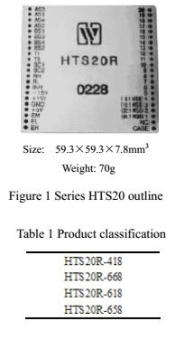
1 FEATURES( Outline is shown in Fig 1, Classifications are shown in Tab 1. )
|
Complete 2-speed system
|

|
|
Programmable speed ratios in coarse/fine channel
|
|
1:8, 1:16, 1:32, 1:64
|
|
Digital output with 3-state latches
|
|
Maximum resolution is 20 bit
|
|
Maximum accuracy is 5 Arcsec
|
2 APPLICATIONS of Synchro to Digital Converters or Resolver to
Digital Converter HTS20 Series Programmable 2-speed SDC/RDC Converters
-
Radar monitoring
-
Tracking navigation
-
Satellite tracking
-
Artificial technology
-
Artillery control
-
Industrial machine control
Other high-accuracy measurement
3 GENERAL DESCRIPTION of Synchro to Digital Converters or
Resolver to Digital Converters HTS20 Series Programmable 2-speed SDC/RDC
Converters
Series HTS20 programmable 2-speed SDC/RDC converter are single module
hybrid integrated circuit packaged in metal case. They internally
contain coarse/fine two way synchro to digital converters or resolver to
digital converters and error correcting logical circuit required by two
way system.
Speed ratios of coarse/fine combination of Series HTS20 products are
1:8, 1:16, 1:32, 1:64,the required speed ratio can be obtained by
external program. It is convenient to use. Two way coarse/fine input
signals are signals of three-wire synchro or four-wire resolver.
Series HTS20 programmable 2-speed SDC/RDC converter output natural
parallel binary codes. Maximum is up to 20bit. They have 3-state
latches.
4 TECHNICAL SPECIFICATIONS of Synchro to Digital Converters or
Resolver to Digital Converters HTS20 Series Programmable 2-speed SDC/RDC
Converters
( Tab 2, Tab 3 )
Table 2 Nominal conditions and recommended operating conditions
|

|
* means that it can be made to order.
|
Table3 Electrical characteristics
|
Characteristics
|
Conditions
|
HTS20R/HTS20S
Business military standard
(Q/HW30925-2006)
|
Units
|
Comments
|
|
Min
|
Max
|
|
Resolution
(optionally controlled by SC1, SC2)
|
speed ratio
1:8
1:16
1:32
1:64
|
-
-
-
-
|
17
18
19
20
|
bit
|
|
|
Accuracy(0°~360°)
|
speed ratio
1:8
1:16
1:32
1:64
|
-
-
-
-
|
40
20
10
5
|
Arc sec
|
|
|
Fine channel tracking velocity
Frequency range
Exciting voltage range(effective value)
Signal voltage range(effective value)
|
400Hz
-
-
-
|
-
50
2
2
|
36
10k
115
90
|
Rev/s
Hz
V
V
|
|
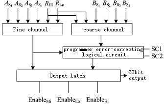
5 CIRCUIT THEORY DIAGRAM of Synchro to Digital Converters or
Resolver to Digital Converters HTS20 Series Programmable 2-speed SDC/RDC
Converters( Fig 2, Fig 3 )
(1) Single speed converter
The principles of operation of single speed converter are shown in fig2., principles are summarized as follows:
Internal differential isolation converts input signals of synchro(resolver) into orthogonal signals:
V1=KE0sinθsinωt , V2=KE 0 cosθsinωt
Where θis analogue input angle.
The two signals are multiplied by digital angle φ of internal up/down
counter in sin/cos multiplier, thus result in error signal:
KE0 sinθcosφsinωt –KE0cosθsinφsinωt=KE0 sin(θ-φ)sinωt
After error magnification, phase demodulator and integrator, the signal
is inputted into VCO. If θ-φ≠0, VCO will output pulse, up/down counter
will count untilθ-φ=0. During this process, converter continuously
tracks changes of input angle.
(2) 2-speed converter
The principles of operation of 2-speed converter are shown in fig3. The
operation of the coarse and fine channel of the 2-speed converter is the
same as above-mentioned single speed, but 2-speed converter consists of
two sets of single speed converter and programmer error logical
circuit. Coarse channel fulfills conversion from 10~12bit logical angle
to digital angle. Fine channel fulfills conversion from 14bit logical
angle to digital angle. digital angles converted by Coarse channel and
Fine channel are inputted into programmer error-correcting logical
circuit respectively. After error processing and correcting, it will
output a 20bit parallel binary digit, which is inputted into output
latch and buffered to output digital angle, fulfilling the entire
conversion.

|
|
Figure2 Functional block diagram
Figure3 Functional block diagram
of single speed converter of 2-speed converter
|
(3) Data transfer method and timing
Outputs of series HTS20 2-speed converters reach 20bit. Through

,

and

which take 3-state control of output latch, 2-speed converter can be easily connected to data bus.
,
and
are all valid at low level. EnableLo controls low 8bits, EnableMi controls middle 8bits, EnableHi controls rest high bits.
Data of series HTS20 2-speed converters are read as follows:
Set

to logical “0”, after 490μm, data in 3-state latch of the converter are
upgraded. It can read data of low 8bits, middle 8bits and high bits
through controlling
,
and
.
Figure 4 Gives timing of reading data when 2-speed converter and 8 bit data bus are connected.
To ensure high-accuracy conversion of 2-speed converter, please pay attention to the following:
-
Amplitudes of input signals of coarse and fine channels should be guaranteed within nominal value 10%.
-
Frequencies of input signals and reference signals of coarse and fine channels should be the specified operating frequencies.
-
Phase shift between input signal and reference signal of coarse
channel and phase between input signal and reference signal of fine
channel should be less than 10°.
-
Wave distortions of input signals and reference signals of coarse and fine channels should be less than 5%.
-
Variation of +5V, ±15V power supply should be guaranteed within ±5%.
6 MTBF DIAGRAM of Synchro to Digital Converters or
Resolver to Digital Converters HTS20 Series Programmable 2-speed SDC/RDC
Converters ( Fig 5 )
|
7 PIN CONFIGURATIONS of Synchro to Digital Converters or
Resolver to Digital Converters HTS20 Series Programmable 2-speed SDC/RDC
Converters ( Fig6, Tab4 )
|

|

|
Figure 5 MTBF vs. temperature Figure 6 Pin out top view
( Note: According to GJB/Z 299B-98, assuming
that ground is in good condition)
|
Table 4 Pin description
|
Pin
|
Mnemonic
|
Description
|
Pin
|
Mnemonic
|
Description
|
|
1
2
3
4
5
6
7
8
9
10
11
12
13
14
15
16
17
18
19
20
21
22
|
As3
As1
As4
As2
Bs1
Bs3
Bs4
Bs2
T1
T2
SC1
SC2
RHi
RLo
Inhibit
-15V
+15V
GND
+5V
|
Fine channel input
Fine channel input
Fine channel input
Fine channel input
Coarse channel input
Coarse channel input
Coarse channel input
Coarse channel input
Adjustment pin for phase shift
between signal and reference
Adjustment pin for phase shift
between signal and reference
Program control pin for coarse
and fine speed ratios
Program control pin for coarse
and fine speed ratios
Input pin for reference high
Input pin for reference low
Inhibit signal
-15V input
+15V input
ground
+5V input
enable middle 8bits data
enable low 8bits data
enable high 4bits data
|
23
24
25
26
27
28
29
30
31
32
33
34
35
36
37
38
39
40
41
42
43
44
|
case
NC
64:1MSB D1
32:1MSB D2
16:1MSB D3
8:1MSB D4
D5
D6
D7
D8
D9
D10
D11
D12
D13
D14
D15
D16
D17
D18
D19
D20
|
Case ground
Not connected
Output of the highest combined digital angle
Output of combined digital angle
Output of combined digital angle
Output of combined digital angle
Output of combined digital angle
Output of combined digital angle
Output of combined digital angle
Output of combined digital angle
Output of combined digital angle
Output of combined digital angle
Output of combined digital angle
Output of combined digital angle
Output of combined digital angle
Output of combined digital angle
Output of combined digital angle
Output of combined digital angle
Output of combined digital angle
Output of combined digital angle
Output of combined digital angle
Output of the least combined digital angle
|
Note:
-
Pin3,7 of HTS20S are not connected.
-
As1,As2, As3, As4 are fine channel input. If synchro is equipped with three wire, As4 is not used.
-
Bs1,Bs2,Bs3,Bs4 are coarse channel input. If synchro is equipped with three wire, Bs4 is not used.
-
RHi, RLo are reference signal input.
Inhibit is inhibit signal which is connected to 5V power supply by pull-up resistor. When Inhibit is logical “0”, inside is inhibited. After 490ns, valid data are outputted and can be read. When is logical “1”, converter restores tracking state, the outputted data are invalid data.
Inhibit
,
and
are three state control pins of data output, which determined the state
of outputted data. When they are logical “1”, data output pin is in
high impedance. When they are logical “0”, After 200ns, data output pin
outputs valid data. Outputted data state doesn’t affect the loop
operation inside converter.
controls low 8bits data,
controls middle 8bits data,
controls the rest high bits data.
T1 and T2 are phase shift adjustment network between coarse/fine channel
signal and reference, circuit types are shown in figure7. By selecting
R,C , it makes phase shift between signal and reference less than
10°.The type of R,C phase shift network can be adjusted according to
advance and lag relation between signal and reference during test. If
adjustment of phase shift is not needed, T1 and T2 are shorted out.

Figure 7 Phase shift adjustment network diagram
SC1,SC2 are speed ratio program control pins of coarse/fine channel.
When used, they are connected to ground by 10kΩ or to +5V voltage. The
truth table is:

Case is case pin.
D1~D20 are Outputs of combined digital angle. D20 is least significant
bit. When speed ratio is 1:8, D4 is most significant bit. When speed
ratio is 1:16, D3 is most significant bit. When speed ratio is 1:32, D2
is most significant bit. When speed ratio is 1:64, D1 is most
significant bit.
8 BIT WEIGHT TABLE of Synchro to Digital Converters or Resolver
to Digital Converters HTS20 Series Programmable 2-speed SDC or RDC
Converters ( Tab 5 )
Table 5 Bit weight table
|
Bit
number
|
Weight (degrees)
|
Bit
number
|
Weight (degrees)
|
Bit
number
|
Weight (degrees)
|
|
1(MSB)
|
180.0000
|
8
|
1.1063
|
15
|
0.011(40sec)
|
|
2
|
90.0000
|
9
|
0.7031
|
16
|
0.0055(20sec)
|
|
3
|
45.0000
|
10
|
0.3516
|
17
|
0.00275(10sec)
|
|
4
|
22.5000
|
11
|
0.1758
|
18
|
0.00138(5sec)
|
|
5
|
11.2500
|
12
|
0.0879
|
19
|
6.88×10⁻⁴(2.5sec)
|
|
6
|
5.6250
|
13
|
0.0439
|
20
|
3.44×10⁻⁴(1.25sec)
|
|
7
|
2.8125
|
14
|
0.0220
|
|
|
9 CONNECTION OF CONVERTER of Synchro to Digital Converters or
Resolver to Digital Converters HTS20 Series Programmable 2-speed SDC or
RDC Converters
±15V,+5V and ground are connected to the corresponding pins of the
converter. Pay attention to the polarity of power supply, or it will
harm device. It is suggested that 0.1μf and 6.8μf by-pass capacitors are
connected between power supplies and ground.
Signal and exciting source are permitted to be connected to S1,S2,S3,S4 and RHi , RLo with 5% error.
Signal input should be in coordination with exciting phase, their phases are as follows:
RHi ~RLo :VRefsinωt
In the case of synchro:
S1~S3: E S1~S3=ERLo~RHisinθsinωt
S3~S2: E S3~S2=ERLo~RHisin(θ+120°)sinωt
S2~S1: E S2~S1=ERLo~RHisin(θ+240°)sinωt
In the case of resolver:
S1~S3: E S1~S3=ERLo~RHisinθsinωt
S2~S4: E S2~S4=ERHi~RLocosθsinωt
Note: input signals in RHi, RLo, S1, S2, S3, S4 are not permitted to connect other pins, or it will damage the device.
Other pins should be connected according to pin definition of the device.
It is suggested that user should inform manufacturer to have device made
to order according to parameters when using non-nominal synchro or
resolver.
10 PACKAGE OUTLINE DIMENTION AND DISCRIPTION of Synchro to
Digital Converters or Resolver to Digital Converters HTS20 Series
Programmable 2-speed SDC/RDC Converter
( Unit: mm) ( Fig 8, Tab 6 )

Figure 8 Package outline drawing
Table 6 Packaging case descriptions
|
Case model
|
Base material
|
Base coat
|
Lid(cap)
material
|
Lid(cap)
coat
|
Lead material
|
Lead coat
|
Sealing
method
|
Comments
|
|
UP5959-44
|
Kovar
(4J29)
|
Ni/Au
|
Fe/Ni alloy
|
Ni/Au
|
Kovar
(4J29)
|
Ni/Au
|
Match sealing
|
|
Note: The temperature of soldered pins does not surpass 300℃ within 10 sec.
11 DESCRIPTIONS OF Synchro to Digital Converters or Resolver to
Digital Converters HTS20 Series Programmable 2-speed SDC/RDC Converters
MODEL NUMBERING ( Fig 9 )

|

|
Figure9 Descriptions of product name
|
Note: When signal voltage and reference voltage(Z) above are not nominal, product name is given as follows:

(for example, reference voltage is 5V, signal voltage is 3V, name denotes 5/3)
Application notes:
-
Polar voltage of power supply should be correct.
-
When exceeding absolute maximum nominal value, it will possibly lead to damage to the device.
-
While assembling, the bottom of the product should be placed close to
the board to avoid damage to the pins. If necessary, take shockproof
measures.
-
When product is ordered, detailed electrical performance specifications should be referred to corresponding business standard.

 X
X


 Gold Supplier