|
Absolute Max. Rating |
|
|
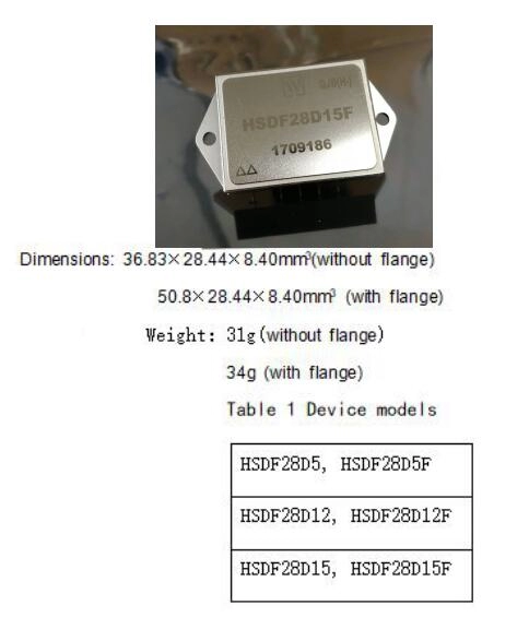
Input voltage:15V~50V Input voltage(Transient,1s):80V Output Power: 22W Storage temperature:-65℃~150℃ |
Mechanical Shock:1500g Lead resistance welding temperature:300℃(15s) Weight(withoutflange/ with flange): 31g/34g Antistatic intensity:2000V |
|
No. |
Items |
Conditions (Testing condition as perTc=25℃,VIN=28V±5%, unless otherwise specified) |
HSDF28D5 HSDF28D5F |
HSDF28D12 HSDF28D12F |
HSDF28D12 HSDF28D12F |
||||||||
|
Min |
Max |
Min |
Max |
Min |
Max |
||||||||
|
1 |
Input Voltage/V |
Low、High、Ambient Temperature |
15 |
50 |
15 |
50 |
15 |
50 |
|||||
|
2 |
Output Voltage/V |
Positive |
Ambient |
4.95 |
5.05 |
11.88 |
12.12 |
14.85 |
15.15 |
||||
|
Negative |
4.80 |
5.20 |
11.80 |
12.20 |
14.80 |
15.20 |
|||||||
|
Positive |
Low/high |
4.925 |
5.075 |
11.82 |
12.18 |
14.80 |
15.20 |
||||||
|
Negative |
4.75 |
5.25 |
11.52 |
12.48 |
14.40 |
15.60 |
|||||||
|
3 |
Output current/A |
VIN=15V~50V |
― |
1.5 |
― |
0.833 |
― |
0.666 |
|||||
|
4 |
Output Power/W |
|
0 |
15 |
0 |
20 |
0 |
20 |
|||||
|
5 |
Output Ripple Voltage/mV |
BW≤6MHz,Io=Full load |
― |
60 |
― |
50 |
― |
60 |
|||||
|
6 |
Line Regulation/mV |
Positive |
VIN=16V~40V,Io=Full |
― |
50 |
― |
50 |
― |
50 |
||||
|
Negative |
― |
50 |
― |
50 |
― |
50 |
|||||||
|
7 |
LoadRegulation/mV |
Positive |
No load to full |
― |
50 |
― |
50 |
― |
50 |
||||
|
Negative |
― |
50 |
― |
50 |
― |
50 |
|||||||
|
8 |
Input current/mA |
Inhibited |
― |
6 |
― |
6 |
― |
6 |
|||||
|
Io=no load |
― |
60 |
― |
60 |
― |
60 |
|||||||
|
9 |
Input Ripple current/mA |
BW≤20MHz,Io=Full load |
― |
60 |
― |
60 |
― |
60 |
|||||
|
10 |
Efficiency/% |
Io=Full load |
73 |
― |
78 |
― |
79 |
― |
|||||
|
11 |
Isolation/MΩ |
Input to output or any pin to case(except pin 7、8)at 500V,Tc=25℃ |
100 |
― |
100 |
― |
100 |
― |
|||||
|
12 |
Inhibit Function |
|
0 |
0.7 |
0 |
0.7 |
0 |
0.7 |
|||||
|
13 |
Under-voltage open voltage/V |
Io=Full Load |
12.0 |
14.8 |
12.0 |
14.8 |
12 |
14.8 |
|||||
|
14 |
Under-voltagecut-off voltage/V |
Io=Full Load |
11.0 |
14.5 |
11.0 |
14.5 |
11 |
14.5 |
|||||
|
15 |
Short Circuit Protection |
|
|
|
|
||||||||
|
16 |
/μF |
Tc=25℃ |
― |
500 |
― |
500 |
― |
500 |
|||||
|
17 |
Io=Full Load |
350 |
500 |
350 |
500 |
350 |
500 |
||||||
|
18 |
Cross Regulation |
One is 30% load, another one is from 30% to 70% load |
― |
500 |
― |
500 |
― |
500 |
|||||
|
19 |
Step Load Response Transient(mV pK) |
50%load→full load →50%load |
― |
400 |
― |
400 |
― |
400 |
|||||
|
20 |
Step Load Response Recovery(μs) |
50%load→full load →50%load |
― |
500 |
― |
500 |
― |
500 |
|||||
|
21 |
Step Line Response Transient(mV pK) |
VIN:16V→40V, VIN:40V→16V,Io=Full load |
― |
800 |
― |
900 |
― |
900 |
|||||
|
22 |
Step Line Response Recovery(μs) |
VIN:16V→40V VIN:40V→16V Io=Full load |
― |
700 |
― |
500 |
― |
500 |
|||||
|
23 |
Start-up Overshoot(mV pK) |
VIN:0→28V, Io=Full load |
― |
25 |
― |
50 |
― |
50 |
|||||
|
24 |
Start-up Delay (ms) |
VIN:0→28V, Io=Full load |
― |
20 |
― |
20 |
― |
20 |
|||||


|
Pin |
Symbol |
Designation |
|
1 |
INH |
Inhibit |
|
2 |
VO+ |
Positive Output |
|
3 |
GNDO |
Output Common |
|
4 |
VO- |
Negative Output |
|
5 |
NC |
No connection |
|
6 |
GNDC |
Case Ground |
|
7 |
GNDI |
Input Common |
|
8 |
VIN |
Positive Input |


|
|
 |
|
Fig. 11 Bottom View |
Fig. 12 Side View |
 |
 |
|
Fig. 13 Bottom View |
Fig. 14 Side View |
|
Symbol |
Unit/mm |
||
|
Min |
Typical |
Max |
|
|
A |
- |
8.4 |
8.90 |
|
A1 |
1.20 |
1.50 |
1.80 |
|
φb |
0.63 |
0.76 |
0.89 |
|
D |
- |
28.44 |
28.94 |
|
E |
- |
36.83 |
37.33 |
|
e |
- |
20.32 |
- |
|
e1 |
- |
5.21 |
- |
|
e2 |
- |
12.83 |
- |
|
e3 |
- |
17.91 |
- |
|
e4 |
|
22.99 |
|
|
e5 |
- |
28.07 |
- |
|
X |
|
50.80 |
51.30 |
|
X1 |
43.45 |
43.95 |
44.45 |
|
P |
3.00 |
3.30 |
3.60 |
|
L |
5.35 |
6.35 |
- |
|
Case Model |
Header |
Header Plating |
Cover |
Cover Plating |
Pin |
Pin Plating |
Seal |
Notes |
|
UPP3728-08t (without flange) |
Cold Rolled Steel(10#) |
Ni |
Kovar (4J42) |
Ni |
Cu-coreCompound |
Ni/Au |
Parallel seam |
Ni Plating is for case ground pin |
|
UPP3728-08j (with flange) |
Cold Rolled Steel(10#) |
Ni |
Kovar (4J42) |
Ni |
Cu–core Compound |
Ni/Au |
Parallel seam |
Ni Plating is for case ground pin |


Fig. 15 Part Numbering Key

Subscribe to our weekly newsletter and receive exclusive offers on products you love!
 X
X


 Gold Supplier