|
· 16 to 40 VDC input, typical 28V |
|
|
· Model HSA15S5 10 to 20V DC output, typical 15V |
|
|
· 5W output power |
|
|
· -55℃ to +125℃ operation |
|
|
· Fully isolated |
|
|
· More than100MΩ(500V DC) isolation |
|
|
· Inhibit function and indefinite short circuit protection |
|
|
· 500kHz operating frequency |
|
|
· Equivalent with Interpoint’s MSA Series |
|
|
· Hermetically sealed metal cases |
Table 1 Product models of HSA28 Series Military Grade DC-DC Converters
|
MODELS |
|
|
SINGLE |
DUAL |
|
HSA28S5(F) HSA28S12(F) HSA28S15(F) HSA28S5R2(F) HSA28S60(F) HSA15S5(F) HSA28S28R5(F) HSA28S3R3(F) HSA28S2R5 HSA28S2R5-A(F) |
HSA28D5(F) HSA28D12(F) HSA28D15(F)
|
The operating principle is that the sampling signal of output voltage, coupled by the opto-coupler, works together with the sampling signal of input loop current to regulate the pulse width of the controller. The double close loop control can create constant voltage output and short circuit protection.
Thick film hybrid integrated techniques provide the HSA28 Series of DC DC converters with reliability levels and optimum miniaturization. The design and manufacturing process of HSA28 Series of converters are in compliance with General Standards of Hybrid Integrated Circuits (MIL-883 DC/DC converters)and detailed standards of manufacturing. Connected to a HFD-CE03 filter, the HSA28 Series of converter can achieve better electromagnetic compatibility (EMC) performance.
ELECTRICAL PERFORMANCE
|
ABSOLUTE MAXIMUM RATINGS · Input Voltage: 40V ( 20V for Model HSA15S5) · Power dissipation: 2.6W · Output power: 5.7W · Lead Soldering Temperature : 300°C (10 sec per lead) · Storage Temperature Range (Case): -55℃~ +125℃ · Inhibit voltage: ≤0.2V |
|
RECOMMENDED OPERATING CONDITIONS · DC Input voltage range :16~ 40V (10~20V for Model HSA15S5 ) · Case Operating Temperature (Tc): –55°C to +125°C |
HSA28S5(F), HSA28S12(F) , HSA28S15(F)
Table 2 Electrical Characteristics(TCASE = -55°C to +125°C, VIN = 28V ± 0.5V, Full Load5, Unless Otherwise Specified)
|
Single output models |
HSA28S5(F) |
HSA28S12(F) |
HSA28S15(F) |
|||||
|
Parameter |
Conditions |
Min |
Max |
Min |
Max |
Min |
Max |
|
|
Output Voltage (V) |
Io=full load |
Ambient temperature high and low temperature |
4.95 4.80 |
5.05 5.20 |
11.88 11.52 |
12.12 12.48 |
14.85 14.40 |
15.15 15.60 |
|
Output Current (A) |
Vin= 16 TO 40 VDC |
- |
1 |
- |
0.417 |
- |
0.333 |
|
|
Output Power (W) |
- |
- |
5 |
- |
5 |
- |
5 |
|
|
Output Ripple Voltage(mV) |
BW=10kHz to 2 MHz Io=full load |
Ambient temperature high and low temperature |
- - |
350 525 |
- - |
200 300 |
- - |
170 250 |
|
Line Regulation (mV) |
VIN = 16 TO 40 VDC,Io=full load |
-- |
50 |
- |
50 |
- |
50 |
|
|
Load Regulation (mV) |
Io=No load to full load |
- |
50 |
- |
50 |
- |
50 |
|
|
Input Ripple Current (mA) |
BW=10kHz-2 MHz Io=full load |
Ambient temperature high and low temperature |
- - |
100 150 |
- - |
100 150 |
- - |
100 150 |
|
Efficiency (%) |
Io=full load |
Ambient temperature high and low temperature |
66 64 |
- - |
70 68 |
- - |
71 69 |
- - |
|
Isolation (MΩ) |
Input to output or any pin to case (except case ground pin) at 500 VDC, TA = 25° C |
100 |
- |
100 |
- |
100 |
- |
|
|
Inhibit Function |
TA = 25° C,Inhibit voltage, output disabled |
have |
have |
have |
||||
|
Protection Function |
TA = 25° C |
have |
have |
have |
||||
|
Start-up Overshoot (mV pk) |
Vin=0 to 28V, Io=full load |
- |
500 |
- |
500 |
- |
500 |
|
|
Start-up Delay (ms) |
Vin=0 to 28V, Io=full load |
- |
75 |
- |
30 |
- |
30 |
|
|
Capacitive Load(μF) |
TA = 25° C, No effect on DC performance |
- |
300 |
- |
500 |
- |
500 |
|
|
Switching Frequency (kHz) |
Io=full load |
400 |
600 |
400 |
600 |
400 |
600 |
|
|
Step Load Response Transient(mV pK) |
50% load -- full load -50% load |
Ambient temperature high and low temperature |
-250 |
250 |
-375 |
375 |
-500 |
500 |
|
-750 |
750 |
-1100 |
1100 |
-1500 |
1500 |
|||
|
Step Load Response Recovery (μs) |
50% load -- full load -50% load |
Ambient temperature high and low temperature |
- |
250 |
- |
500 |
- |
500 |
|
- |
1500 |
- |
3000 |
- |
3500 |
|||
|
Step Line Response Transient (mV pK) |
Vin=16~40V, Io=full load Vin=40~16V, Io=full load |
-500 |
500 |
-1000 |
800 |
-500 |
500 |
|
|
Step Line Response Recovery (μs ) |
Vin=16~40V, Io=full load Vin=40~16V, Io=full load |
- |
500 |
- |
1300 |
- |
1300 |
|
|
- |
900 |
|||||||
|
Load Fault Short Circuit recovery(ms) |
Io fromshort circuit to full load |
- |
75 |
- |
30 |
- |
30 |
|
Notes to Specifications:
· The step load transition time should be greater than or equal to 10µs.
· The step line transition time should be greater than or equal to 10µs.
· Recovery time is measured from application of the transient to point at which VOUT is within 1% of VOUT at final value.
HSA28S5R2(F), HSA28S60(F), HSA15S5(F)
Table 3 Electrical Characteristics: (TCASE = -55°C to +125°C, VIN = 28V ± 0.5V, Full Load5, Unless Otherwise Specified)
|
Single output models |
HSA28S5R2(F) |
HSA28S60(F) |
HSA15S5(F) |
|||||
|
Parameter |
Conditions |
Min |
Max |
Min |
Max |
Min |
Max |
|
|
Output Voltage (V) |
Io=full load |
Ambient temperature high and low temperature |
5.15 |
5.25 |
59.1 |
60.9 |
5.0 |
5.1 |
|
4.99 |
5.41 |
56.0 |
64.0 |
4.9 |
5.2 |
|||
|
Output Current(A) |
VIN= 16 TO 40 VDC( VIN= 10 TO 20 VDC) |
- |
0.962 |
- |
0.020 |
- |
0.8 |
|
|
Output Power(W) |
- |
- |
5.2 |
- |
5.2 |
- |
5 |
|
|
Output Ripple Voltage (mV) |
BW=10 kHz to 2 MHz (BW≤20MHz) Io=full load |
Ambient temperature |
- |
350 |
- |
300 |
- |
50 |
|
high and low temperature |
- |
525 |
||||||
|
Voltage Regulation (mV) |
VIN= 16 TO 40 VDC,( VIN= 10 TO 20 VDC) Io=full load |
- |
50 |
- |
300 |
- |
50 |
|
|
Load Regulation(mV) |
Io=No load to load |
- |
50 |
- |
300 |
- |
50 |
|
|
Input Ripple Current(mA) |
BW=10kHzto 2MHz, Io=full load |
Ambient temperature high and low temperature |
- |
100 |
- |
90 |
- |
- |
|
- |
150 |
- |
- |
- |
- |
|||
|
Efficiency (%) |
Io=full load |
Ambient temperature high and low temperature |
66 |
- |
70 |
- |
72 |
- |
|
64 |
- |
65 |
||||||
|
Isolation(MΩ) |
Input to output or any pin to case (except case ground pin) at 500 VDC, TA = 25° C |
100 |
- |
100 |
- |
100 |
- |
|
|
Inhibit Function |
TA = 25° C,Inhibit voltage, output disabled |
have |
have |
have |
||||
|
Protection Function |
TA = 25° C |
|||||||
|
Start-up Overshoot (mV pk) |
Vin=16 to 40V, Io=full load |
- |
500 |
- |
- |
- |
- |
|
|
Start-up Delay (ms) |
Vin=16 to 40V, Io=full load |
- |
75 |
- |
- |
- |
25 |
|
|
Capacitive Load (μF) |
TA = 25° C, No effect on DC performance |
- |
300 |
- |
- |
- |
- |
|
|
Switching Frequency(kHz) |
Io=full load |
400 |
600 |
400 |
600 |
- |
- |
|
|
Step Load Response Transient(mV pK) |
50% load -- full load -50% load |
Ambient temperature high and low temperature |
-250 |
250 |
- |
- |
- |
- |
|
-750 |
750 |
|||||||
|
Step Load Response Recovery (μs) |
50% load -- full load -50% load |
Ambient temperature high and low temperature |
- |
250 |
- |
- |
- |
- |
|
- |
1500 |
|||||||
|
Step Line Response Transient (mV pK) |
Vin=16~40V, Io=full load Vin=40~16V, Io=full load |
-500 |
500 |
- |
- |
- |
- |
|
|
Step Line Response Recovery (μs ) |
Vin=16~40V, Io=full load Vin=40~16V, Io=full load |
- |
500 |
- |
- |
- |
- |
|
|
- |
900 |
|||||||
|
Load Fault Short Circuit recovery ms) |
Io fromshort circuit to full load |
- |
75 |
- |
- |
- |
- |
|
Notes to Specifications:
· The step load transition time should be greater than or equal to 10µs.
· The step line transition time should be greater than or equal to 10µs.
· Recovery time is measured from ap plication of the transient to point at which VOUT is within 1% of VOUT at final value.
HSA28S28R5(F), HSA28S3R3(F)
Table 4 Electrical Characteristics: (TCASE = -55°C to +125°C, VIN = 28V ± 0.5 V, Full Load5, Unless Otherwise Specified)
HSA28S2R5 , HSA28S2R5-A(F)
|
Single output models |
HSA28S28R5(F) |
HSA28S3R3(F) |
||||
|
Parameter |
Conditions |
Min |
Max |
Min |
Max |
|
|
Output Voltage (V) |
Io=full load |
Ambient temperature |
28.2 |
29 |
3.20 |
3.40 |
|
high and low temperature |
27.7 |
29.3 |
3.15 |
3.45 |
||
|
Output Current (A) |
VIN= 16 TO 40 VDC |
- |
0.2 |
0 |
1.2 |
|
|
Output Power (W) |
- |
- |
5.7 |
- |
4.5 |
|
|
Output Ripple Voltage (mV) |
BW=10 kHz to 2 MHz Io=full load |
- |
60 |
- |
50 |
|
|
Line Regulation (mV) |
VIN= 16 TO 40 VDC,( VIN= 10 TO 20 VDC) Io=full load |
Ambient temperature |
- |
28 |
- |
50 |
|
high and low temperature |
- |
100 |
||||
|
Load Regulation(mV) |
Io=No load to load |
Ambient temperature |
- |
140 |
- |
50 |
|
high and low temperature |
- |
100 |
||||
|
Efficiency (%) |
Io=full load |
75 |
- |
70 |
- |
|
|
Isolation (MΩ) |
Input to output or any pin to case (except case ground pin) at 500 VDC, TA = 25° C |
100 |
- |
100 |
- |
|
|
Inhibit Function |
TA = 25° C,Inhibit voltage, output disabled |
have |
have |
|||
|
Protection Function |
TA = 25° C |
|||||
|
Start-up Overshoot (mV pk) |
Vin=0 to 28V, Io=full load |
- |
- |
|||
|
Start-up Delay(ms) |
Vin=0to 28V, Io=full load |
- |
5 |
- |
5 |
|
|
Capacitive Load(μF) |
TA = 25° C, No effect on DC performance |
- |
- |
- |
- |
|
|
Switching Frequency (kHz) |
Io=full load |
400 |
600 |
- |
- |
|
Table 5 Electrical Characteristics: (TCASE = -55°C to +125°C, VIN = 28V ± 0.5V, Full Load5, Unless Otherwise Specified)
|
Single output models |
HSA28S2R5 |
HSA28S2R5-A(F) |
||||
|
Parameter |
Conditions |
Min |
Max |
Min |
Max |
|
|
Output Voltage (V) |
Io=full load |
Ambient temperature |
2.40 |
2.60 |
2.40 |
2.60 |
|
high and low temperature |
2.35 |
2.65 |
2.35 |
2.65 |
||
|
Output Current (A) |
VIN= 16 TO 40 VDC |
0 |
1 |
0 |
2 |
|
|
Output Power (W) |
- |
- |
3 |
- |
5.5 |
|
|
Output Ripple Voltage (mV) |
BW=10 kHz to 2 MHz Io=full load |
- |
80 |
- |
35 |
|
|
Line Regulation (mV) |
VIN= 16 TO 40 VDC,( VIN= 10 TO 20 VDC) Io=full load |
Ambient temperature |
- |
50 |
- |
10 |
|
high and low temperature |
- |
100 |
- |
20 |
||
|
Load Regulation (mV) |
Io=No load to load |
Ambient temperature |
- |
50 |
- |
50 |
|
high and low temperature |
- |
100 |
- |
70 |
||
|
Efficiency (%) |
Io=full load |
60 |
- |
68 |
- |
|
|
Isolation (MΩ) |
Input to output or any pin to case (except case ground pin) at 500 VDC, TA = 25° C |
100 |
- |
100 |
- |
|
|
Inhibit Function |
TA = 25° C,Inhibit voltage, output disabled |
have |
have |
|||
|
Protection Function |
TA = 25° C |
|||||
|
Start-up Overshoot (mV pk) |
Vin=0 to 28V, Io=full load |
- |
- |
- |
- |
|
|
Start-up Delay (ms) |
Vin=0to 28V, Io=full load |
- |
5 |
- |
5 |
|
|
Capacitive Load (μF) |
TA = 25° C, No effect on DC performance |
- |
- |
- |
- |
|
|
Switching Frequency(kHz) |
Io=full load |
- |
- |
- |
- |
|
|
|
HSA28D5(F), HSA28D12(F) , HSA28D15(F)
Table 6 Electrical Characteristics: (TCASE = -55°C to +125°C, VIN = +28V ± 0.5V, Full Load5, Unless Otherwise Specified)
|
Dual output models |
HSA28D5(F) |
HSA28D12(F) |
HSA28D15(F) |
|||||||
|
Parameter |
Conditions |
Min |
Max |
Min |
Max |
Min |
Max |
|||
|
Output Voltage (V) |
Io1= Io2= full load |
Ambient temperature |
4.95 |
5.05 |
11.88 |
12.12 |
14.85 |
15.15 |
||
|
high and low temperature |
4.80 |
5.20 |
11.52 |
12.48 |
14.40 |
15.60 |
||||
|
Ambient temperature |
-5.10 |
-4.90 |
-12.24 |
-11.76 |
-15.30 |
-14.70 |
||||
|
high and low temperature |
-5.25 |
-4.75 |
-12.96 |
-11.04 |
-16.20 |
-13.80 |
||||
|
Output Current (A) |
VIN= 16 TO 40 VDC |
- |
0.5 |
- |
0.208 |
- |
0.167 |
|||
|
Output Power (W) |
- |
- |
5.23 |
- |
5.3 |
- |
5.3 |
|||
|
Output Ripple Voltage (mV) |
BW=10 kHz to 2 MHz(BW≤20MHz) Io1= Io2= full load |
Ambient temperature |
- |
150 |
- |
140 |
- |
150 |
||
|
high and low temperature |
- |
300 |
- |
250 |
- |
250 |
||||
|
Ambient temperature |
- |
150 |
- |
140 |
- |
150 |
||||
|
high and low temperature |
- |
300 |
- |
250 |
- |
250 |
||||
|
Line Regulation (mV) |
VIN= 16 TO 40 VDC, Io1= Io2= full load |
+Vout |
- |
25 |
- |
50 |
- |
50 |
||
|
-Vout |
- |
75 |
- |
180 |
- |
180 |
||||
|
Load Regulation (mV) |
Io1= Io2=No load to full load |
+Vout |
- |
50 |
- |
50 |
- |
50 |
||
|
-Vout |
- |
200 |
- |
200 |
- |
200 |
||||
|
Efficiency (%) |
Io1= Io2=full load |
Ambient temperature |
68 |
- |
69 |
- |
70 |
- |
||
|
high and low temperature |
65 |
- |
67 |
- |
68 |
|
||||
|
Isolation (MΩ) |
Input to output or any pin to case (except case ground pin) at 500 VDC, TA = 25° C |
|
100 |
- |
100 |
- |
100 |
|||
|
Inhibit Function |
TA = 25° C,Inhibit voltage, output disabled |
have |
have |
have |
||||||
|
Protection Function |
TA = 25° C |
|||||||||
|
Start-up Overshoot (mV pk) |
Vin=0 to 28V, Io1=Io2=full load |
Ambient temperature |
- |
500 |
- |
500 |
- |
500 |
||
|
high and low temperature |
- |
750 |
- |
750 |
||||||
|
Ambient temperature |
- |
500 |
- |
500 |
||||||
|
high and low temperature |
- |
750 |
- |
750 |
||||||
|
Start-up Delay (ms) |
Vin=0 to28V, Io1=Io2=full load |
- |
25 |
- |
30 |
- |
25 |
|||
Table 6 Electrical Characteristics (to be continued)
|
Capacitive Load (μF) |
TA = 25° C, No effect on DC performance |
- |
10 |
- |
100 |
- |
10 |
|
|
Switching Frequency(kHz) |
Io=full load |
400 |
600 |
400 |
600 |
400 |
600 |
|
|
Step Load Response Transient(mV pK) |
50% load to full load or full load to 50% load, Each Vout has balanced load |
Ambient temperature |
-150 |
150 |
-450 |
450 |
-450 |
450 |
|
high and low temperature |
-500 |
500 |
-1400 |
1400 |
-1400 |
1400 |
||
|
Ambient temperature |
-150 |
150 |
-450 |
450 |
-450 |
450 |
||
|
high and low temperature |
-500 |
500 |
-1400 |
1400 |
-1400 |
1400 |
||
|
Step Load Response Recovery (μs) |
50% load to full load or full load to 50% load, Each Vout has balanced load |
Ambient temperature |
- |
100 |
- |
500 |
- |
500 |
|
high and low temperature |
- |
1000 |
- |
4500 |
- |
4500 |
||
|
Ambient temperature |
- |
100 |
- |
500 |
- |
500 |
||
|
high and low temperature |
- |
1000 |
- |
4500 |
- |
4500 |
||
|
Step Line Response Transient (mV pK) |
Vin=16~40V, Io1= Io2=full load |
-750 |
750 |
-500 |
500 |
-1500 |
1500 |
|
|
-500 |
500 |
-1000 |
1000 |
|||||
|
Step Line Response Recovery (μs ) |
Vin=16~40V, Io1= Io2=full load |
- |
1200 |
- |
750 |
- |
1200 |
|
|
Load Fault Short Circuit recovery (ms) |
Io1= Io2 short circuit to full load |
|
|
- |
2000 |
|
|
|
|
|
|
- |
50 |
- |
30 |
- |
50 |
|
· The step load transition time should be greater than or equal to 10µs.
· The step line transition time should be greater than or equal to 10µs.
· Recovery time is measured from application of the transient to point at which VOUT is within 1% of VOUT at final value.
(1) Single output model HSA28S5
|
|
|
|
Figure 2 Efficiency (OUTPUT POWER) |
Figure 3 STEP LINE RESPONSE |
|
|
|
|
Figure 4 STEP LOAD RESPONSE |
Figure 5 Start-up overshoot/ delay |
(2) Dual output model HSA28D5
 |
 |
|
Figure 6 Efficiency (OUTPUT POWER) |
Figure 7 Input STEP LINE RESPONSE |
 |
 |
|
Figure 8 STEP LOAD RESPONSE |
Figure 9 Start-up overshoot/ delay |
 |
|
|
TEMPERATURE (℃) |
TEMPERATURE (℃) |
|
Figure10 Model HSA28 S15 |
Figure 11 Model HSA28D15 |
 |
 |
 |
|
Figure12 Application Connection Diagram for Single output models |
Figure13 Application Connection Diagram for Dual output models |
Figure14 Inhibit Drive connection Diagram for Single Output Models |
 |
 |
 |
|
Figure15 Inhibit Drive connection Diagram for Dual Output Models |
Figure16 Single Output Converter with EMI Filter Connection Diagram |
Figure17 Dual Output Converter with EMI Filter connection Diagram |


Figure18 Package Outline
Table 6 Case Materials
|
Case Model |
Header |
Header Plating |
Cover |
Cover Plating |
Pin |
Pin Plating |
Sealing Style |
Notes |
|
UPP2727-08f |
Cold Rolled Steel |
Nickel/Gold |
Iron/Nickel Alloy |
Nickel/Gold |
Copper Compound |
Nickel/Gold |
Compression Seal |
Nickel plating is for pin8. |
|
|
|
|
Figure19 Pin Out Bottom View |
|
|
|
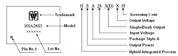
Figure 20 Part Numbering Key |
Application Notes:

Subscribe to our weekly newsletter and receive exclusive offers on products you love!
 X
X


 Gold Supplier