33W  Non-isolated Point of Load DC to DC Converters (POL)

Sales 33W Non-isolated Point of Load DC to DC Converters (POL)

  • Output Voltage (V) : 0.8V-3.3V
  • Input DC Voltage (V) : 4.5V~5.5V
  • Max. Output Power (W) : 33W

Product Detail  

1 Features of HNTA0510S Non-isolated Point of Load DC/DC Converters (POL)

High reliability 

Low voltage input:4.5V~5.5V,Typical 5V
High conversion efficiency
Output Power PO:33W
Operating temperature Tc:-55℃~+125℃ 
Low start-up current
No output overshoot 
Inhibit function          
Output over current and short circuit protection
Maximum power density:108W/in3
Hermetically sealed metal case


2. Scope of application of HNTA0510S Non-isolated Point of Load DC to DC Converters (POL)

High-reliability electronic system for ground, vehicle, radar, aviation, and aerospace, etc.


3. Description of HNTA0510S Non-isolated Point of Load DC to DC Converters (POL)

The HNTA0510S is a highly reliable, output voltage adjustable non-isolated DC-DC converters with BUCK circuit topology and pulse width modulation principle. The output sampling voltage is directly feedbacked to modulate the pulse width to achieve closed-loop control to meet the stability of the voltage output requirements. By changing the external resistance method to achieve the output voltage 0.8V-3.3V adjustable. The series of products are made by the thick-film hybrid integrated production process, metal sealed the package. The design and manufacturing process of HNTA0510S Series converters are in compliance with MIL-PRF-38534.

4. Technical Specifications of HNTA0510S Non-isolated Point of Load DC to DC Converters (POL)

Table 2 Rated conditions and recommended operating conditions

Absolute Max. Rating

Input voltage:4.5V~5.5V

Input voltage(Transient,1s):5.8V

Output Power:35 W

Storage temperature:-65℃~150℃

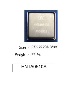
Mechanical Shock:1500g

Lead temperature:300℃(10s)

Weight:17.5 g


Table 3 Electrical characteristics

Items

Sym

Conditions

(Unless other wise,

VI=5V,-55℃≤TC≤125℃)

A Group

Limited

Unit

Min

Max

Output voltage

Vo

VI=5V,IO=10A

1,2,3

0.780

0.820

V

VI=5V,IO=10A

2.437

2.563

VI=4.5V~5.5V,IO=10A

3.217

3.383

Output current

Io

VI=4.5V~5.5V

1,2,3

-

10

A

Output ripple voltage

(Peak-peak)

VR

Vo=3.3V,IO=10A,BW =6MHz

1,2,3

-

80

mV

Current regulation

SI

Vo=3.3V,IO=0→10A

1,2,3

-

60

mV

Input current

II

Null,Inhibit connect Input G

1,2,3

-

3

mA

Null,Inhibit open

1,2,3

-

80

efficiency

η

Vo=3.3V,Io=10A

1,2,3

91

-

%

Insulation resistance

RI

TA=25℃,impose 500V DC voltage between case and any pin (Expect pin 9)

1

100

-

Short circuit power consumption

PD

Output short

1,2,3

-

3

W

Capacitive load

ab

CL

TA=25℃,Vo=3.3V,Io=10A

4

-

5000

μF

switching frequencyb

fs

Vo=3.3V,Io=10A

4,5,6

240

350

kHz

Start-up Overshoot(peak)

VTO

Output voltageVI:0→5V,Vo=3.3V,IO=10A

4,5,6

-

40

mV

Start-up Delay

tTR

Output voltageVI:0→5V,Vo=3.3V,IO=10A

4,5,6

-

8

ms

Notes:

a  Capacitive load may be any value from 0 to the maximum limit with on influence to DC performance.

b  This parameter shall be guaranteed by design and tested only when there is qualification test and design or process change.

c  Load step transition time shall be more than 10μs, connect 100μF capacitor between positive input and ground.

d  Recovery time means the time that step start-up  until the output voltage comes back to the ±1% of the typical value.


5. Circuit block diagram of HNTA0510S Non-ioslated Point of Load DC to DC Converters (POL)


Fig 2 HNTA0510S circuit block diagram
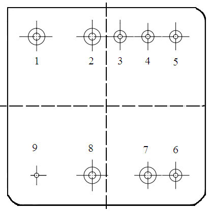
6. Typical Characteristic Curve (Testing condition as per TC=25℃, VIN=5V±0.15V,unless otherwise specified) of HNTA0510S Non-isolated Point of Load DC to DC Converters (POL)


Fig 3 HNTA0510S Efficiency

Fig 4 HNTA0510S Load

Fig 5 HNTA0510S Overshoot/Start-up Delay


7. MTBF Curve of HNTA0510S Non-isolated Point of Load DC to DC Converters (POL)


Fig 6  MTBF Temperature Curve(HNTA0510S)

8. Pin Designations of HNTA0510S Non-isolated Point of Load DC to DC Converters (POL)


Figure 7 Bottom View

Table 4 Pin Designation

Pin

Symbol

Designation

Pin

Symbol

Designation

1

VI

Positive input

6

Trim

Output Trimming

2

GND

Common GND

7

GND

Common GND

3

INH

Inhibit

8

Vo

Positive output

4

Track

Track

9

GNDC

Case GND

5

Sense+

Output positive terminal


9. Typical Connection Diagram of HNTA0510S Non-isolated Point of Load DC to DC Converters (POL)


C1=100μF;C2=10μF;C3=0.1μF   C1、C2、C3 are chip capacitors
Fig 8  Connection Diagram
In fig 8,By adjusting the external resistor Rtr,can achieve different output voltage,Rtr and VO relationship is shown as follow:


Vo(V)

Rtr(kΩ) Reference

3.3

3.3

2.6

6.55

2.5

7.25

0.8

None


Fig 9 Inhibit Driver Circuit Diagram
The start-up delay (roughly 10ms when C=0.01uF) can be enlonged by adjusting the external capacitor.

10. Package Specifications of HNTA0510S Non-isolated Point of Load DC to DC Converters (POL)


Fig 10  Bottom View and Side View
Table 5  Package Outline

Symbols

Unit/mm

Minimum

Nominal

Maximum

A

-

-

7.20

Фb1

0.51

-

0.77

Фb2

0.87

-

1.13

D

-

-

27.57

E

-

-

27.57

e a

3.71

4.01

4.31

e1 a

7.32

7.62

7.92

e2 a

3.51

3.81

4.11

e3 a

18.55

19.05

19.55

L

4.05

-

-


Table 6  Case Materials

Case Model

Header

Header Plating

Cover

Cover Plating

Pin

Pin Plating

Sealing

Notes

PP2727-09B

Cold Rolled Steel

Au

Steel (SPCC-SD)

Ni

Copper –core Compound

Au

Compression


11. Ordering Information of HNTA0510S Non-isolated Point of Load DC to DC Converters (POL)


Fig 11 Part Numbering Key

Application Notes:

☆  Both positive and negative terminals for power supply shall be correctly connected when power is applied so as to avoid permanent damage to the device.
☆  Testing position shall be the root of the pin of the device when the electrical characteristic is measured.
☆  The baseplate of the device shall be closely attached to the circuit board during device mounting so as to avoid the damage on pins. The shockproof actions shall be adopted when necessary.
☆  Pins shall not be bended to avoid the glass insulator cracking and case leaking.
☆  Pins at inhibit terminal shall be hung in the air during no operation.
☆  When ordering this device,the detail electrical specification shall be based on relevant standards. While data offered in this document shall be for reference only.


Leave A Message
If you are interested in our products and want to know more details,please leave a message here,we will reply you as soon as we can.
X

Home

Supplier

Leave a message

Leave a message

If you are interested in our products and want to know more details,please leave a message here,we will reply you as soon as we can.