|
Internal differential isolation conversion |
 |
|
16-bit resolution |
|
|
Accuracy: 2 angular minutes |
|
|
Three-state latch output |
|
|
High continuous tracking speed |
|
|
36-wire salt fog resistant metal sealed DDIP package |
|
| Pin-To-Pin compatible with Model SDC14560 of DDC company |
| Absolute max. rated value | Logical supply voltage VL: +7V |
| Supply voltage Vs: ± 17.5V | |
| Signal voltage V1: rated value ±20% | |
| Reference voltage VRef: rated value ±20% | |
| Operating frequency f: rated value ±20% | |
| Storage temperature Tstg: -65~150℃ | |
| Recommended operating conditions | Logical supply voltage VL: 5±0.5V |
| Supply voltage Vs: 15± 0.75V | |
| Signal voltage V1: rated value ±10% | |
| Reference voltage VRef: rated value ±20% | |
| Operating frequency f: rated value ±20% | |
| Range of operating temperature (TA): -55℃~125℃ |
| Parameter | Conditions | HSDC14569 Series | |
| (VS=15V, VL=+5V) | Military standard (Q/HW20725-2006) | ||
| Min. | Max. | ||
| Resolution | Binary system parallel digital code | 16 bits | — |
| Accuracy | ± 10% of signal voltage, reference voltage and fluctuation range of operating frequency | -2 angular minutes | +2 angular minutes |
| Range of reference frequency | — | 50Hz | 2600Hz |
| Range of reference voltage | — | 2V | 115V |
| Reference input impedance | — | 4.4kΩ | 129.2 kΩ |
| Range of signal voltage | — | 2V | 90V |
| Signal input impedance | — | 4.4kΩ | 102.2 kΩ |
| Signal/reference phase shift | — | —70° | +70° |
| Input logic level | — | Logic “1” ≥3.3V | Logic “0” ≤0.8V |
 input input
|
— | 0 | 0.8V |
 input input
|
— | 0 | 0.8V |
 input input
|
— | 0 | 0.8V |
| Output logic level | — | Logic “1” ≥3.3V | Logic “0” ≤0.8V |
| Digital angle code output | — | Logic “1” ≥3.3V | Logic “0” ≤0.8V |
| Converting busy signal (CB) output | — | 200ns | 600ns |
| Fault detection Bit output | — | Logic “0” indicates fault |
|
| Loading capacity | — | — | 3TTL |
| Tracking speed | — | — | 2.5rps |
| Acceleration constant | — | — | 12500 |
| Settling time | — | — | 850ms |
| Angular velocity voltage (Vel) output | — | —10V | +10V |
| Current | VS=+15V | — | 10mA |
| VS =—15V | 15 mA | ||
| VL=+15V | 20 mA | ||
|
The input signal of synchro (or resolver) is converted into the orthogonal signal through the internal differential isolation: Vsin=KE0sin (ωt+α) sinθ (sin) Vcos=KE0sin (ωt+α) cosθ (cos) Where, θ is the analog input angle. |
 Fig.2 Curve of step response |
 logic low, the output data is valid, and the converter realizes data transfer through . After Inhibit is released, the system will automatically generate a pulse with width equal to the busy pulse for data updating.
 |
(2) Bust mode: At the rising edge of Busy pulse, the three-state reversible counter counts; at the descending edge of Busy pulse, it internally generates a latch pulse with a width equal to Busy pulse for updating the data of three-state latch, the time sequence of data transfer is shown in Fig.4, in other words, after 600ns of Busy logic low, the stable transfer of data is valid. In the asynchronous reading mode, the Busy output is CMOS-level pulse train. The width of its high and low level depends on operating frequency and rotational speed of the selected device. |
|

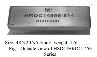
7. MTBF curve (Fig.5) of Synchro to Digital Converters or Resolver to Digital Converters (HSDC/HRDC1459 Series) Fig.5 MTBF-temperature curve |
8.Pin designation (Fig.6, Table 3) of Synchro to Digital Converters or Resolver to Digital Converters (HSDC/HRDC1459 Series)") Fig.6 Pin designation (Bottom view) |
| Pin | Symbol | Meaning | Pin | Symbol | Meaning |
| 1 | S1 | Resolver input S1 (or synchro input S1) | 25 |
|
Digital Enabled control of lower 8 bits |
| 2 | S2 | Resolver input S2 (or synchro input S2) | 26 |

|
Digital Enabled control of higher 8 bits |
| 3 | S3 | Resolver input S3 (or synchro input S3) | 27 | RIPCLK | Zero-bit signal output |
| 4 | S4 | Resolver input S4 (leave unconnected) | 28 | VL | +5V power supply |
| 5月18日 | D1-D14 | Digital output 1(MSB)-14 | 29 | GND | Ground |
| 19 | RHi | High end of reference signal input | 30 | NC | No connection |
| 20 | RL | Low end of reference signal input | 31 | -VS | -15V Power supply |
| 21 | D15 | Digital output 15 | 32 | VS | +15V Power supply |
| 22 | D16 | Digital output 16 (LSB) | 33 | Inhibit | Static signal input |
| 23 | Vel | Angular velocity voltage signal output | 34 |
bit |
Fault detection bit output |
| 24 | CB | Busy signal output | 35-36 | NC | No connection |
| Notes: D1~D16 | Parallel binary system digital angle code output end |
| S1, S2, S3, S4 | Signal input of Resolver (or synchro) |
| RHi | High end of reference signal input |
| RL | Low end of reference signal input |
Lower
8-bit digit enabled signal input, this pin is the logic input pin of
data gating control, its function is to carry out three-state control
externally on the lower 8-bit output data of the converter. Low level is
valid, the lower 8-bit output data of the converter occupies the data
bus; At high level, the pin of lower 8-bit output data is in high
resistance state, and the device does not occupy the data bus. Enable
and release delay time is 600ns(max).
higher
8-bit digit enabled signal input, this pin is the logic input pin of
data gating control, its function is to carry out three-state control
externally on the higher 8-bit output data of the converter. Low level
is valid, the higher 8-bit output data of the converter occupies the
data bus; At high level, the pin of higher 8-bit output data is in high
resistance state, and the device does not occupy the data bus. Enable
and release delay time is 600ns(max).
Inhibit static
signal input, this pin is the input pin of control logic, its function
is to output data externally to the converter to realize optional
latching or bypass control. At high level, the output data of the
converter directly outputs without latching; at low level, the output
data of the converter is latched, the data is not updated, but the
internal loop is not interrupted, and tracking is operating all the
time, Inhibit has connected pull-up resistance internally. After 600ns (max) delay of
descending edge of static signal, the data becomes stable (whether the
device occupies the data bus, i.e. when does it output the data depends
on the state of and ).
CB “Busy” signal output, this signal indicates whether the binary code
output of the converter is valid or not. When the change of angle input
reaches 0.33 angular minute, CB end outputs a positive pulse with a
width of 400ns(typical). When CB is at high level, it indicates the
converter is carrying out data conversion, the data output at this time
is invalid; after 600ns (max) delay of descending edge of CB signal, the
data becomes stable and the updated data output at this time is valid.
bit fault
detection bit output, high level indicates normal operation of the
converter, in the event that the signal wire is broken or the converter
fails to track normally, this bit changes into low level from high
level.
RIPCLK zero-bit signal input, when the output data increment to all “0”
from all “1” or decrement from all “1” from all “0”, a positive pulse
with a width of 200us is output.
VL, +VS, -VS Incoming terminal of power supply
GND Ground wire incoming terminalReference signals are connected to RHi
and RLo. In the case of synchro, signals are connected to S1, S2, and
S3 as per the following conventions.
Notes:


 shall all be connected as described for the above data transfer.

10. Connection diagram for typical application (Fig. 7) of Synchro to Digital Converters or Resolver to Digital Converters (HSDC/HRDC1459 Series) |
11. Package specifications (unit: mm) (Fig. 8, Table 5) of Synchro to Digital Converters or Resolver to Digital Converters (HSDC/HRDC1459 Series) |
 |
 |
|
Fig. 7 Connection diagram for typical application |
Fig.8 Outside view and dimensions of package |
|
Case model |
Header |
Header plating |
Cover |
Covering plating |
Pin material |
Pin plating |
Sealing style |
Notes |
|
UP4820-36A |
4J42 |
Ni plating |
4J42 |
Chemical Ni plating |
4J42 |
Au plating |
Matched seal |
Header plus three solid glass beads |


Subscribe to our weekly newsletter and receive exclusive offers on products you love!
 X
X


 Gold Supplier