Product Detail
Optical communication substrate
I. Overview
Using semiconductor thin film vacuum evaporation, sputtering, electroplating, photolithography, laser trimming, scribing and other processes, pattern metallization on the surface of the ceramic substrate, while integrating resistors, capacitors, inductors, etc., to produce circuit substrates with specific functions , With electrical connection, physical support, heat dissipation and other functions, used in the base substrate of the optical module.
2. Product features
High precision and high reliability
Three, technical indicators
Material: AlN/Al2O3/multilayer AlN-HTCC/quartz.
Accuracy: line width/line spacing accuracy ±2.5um.
Metalization: Ti, Ni, Pt, Au, TaN resistance, prefabricated AuSn film, etc.; meets the requirements of gold wire bonding, AuSn/BiSn welding, and conductive adhesive bonding.
Others: Wrap around on the side, through holes (through hole resistance less than 50 milliohms), solid holes (AlN+W filled).
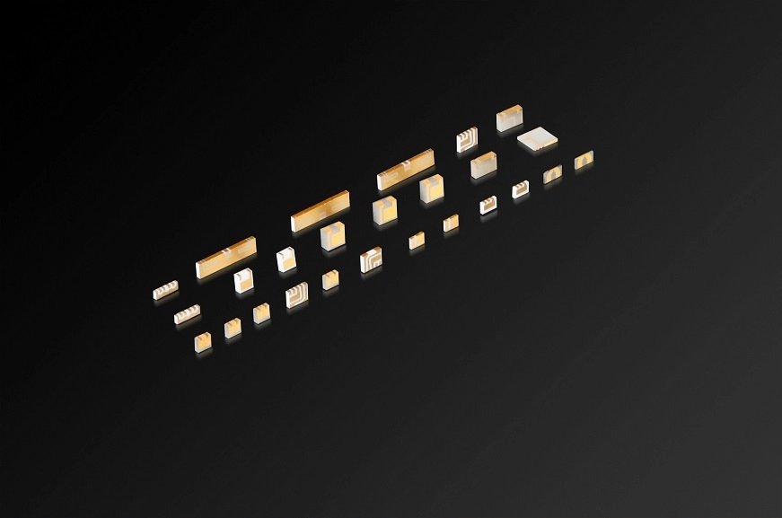
Four, typical products
Conventional base substrates, side products, gold tin products, multilayer substrates + thin film metallization.
Five application areas
TOSA, ROSA, SFP, QSFP, CFP, PON and other optical modules.

 X
X


 Gold Supplier