|
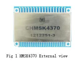
Replacement with MSK4370 of MSK Company |
 |
|
Continuous output current: 10A |
|
|
Motor power voltage: 500V |
|
|
Torque control of four-quadrant |
|
|
60/120 phase selection |
|
|
Inhibition function |
| No. | Characteristic | ( Unless other condition,Vcc=15V±5% | HMSK4370 | Unit | ||
| VS=-15V±5%,VS=28V±5% | ||||||
| -55℃≤Tc≤125℃) | A group | min | max | |||
| 1 | +15V power current/ICC | Speed control GND,empty load,Efficient HALL signal,frequency:40Hz,VH≥3V,VL≤0.8V | 1 | - | 150 | mA |
| -15V power current /IEE | 1 | - | 60 | |||
| 2 | Clock frequency/fcp | Efficient HALL signal,frequency:40Hz,VH≥3V,VL≤0.8V | 4\5\6 | 14 | 20 | KHZ |
| 3 | Reference voltage/VREF | RREF=430Ω | 1\2\3 | 5.82 | 6.57 | V |
| 4 | Control voltage transconductance/gm | Efficient HALL signal,frequency:40Hz,efficient current control setup | 4 | 0.75 | 1.25 | A/V |
| 5 | Bias current/IOO | Efficient HALL signal,frequency:40Hz,VH≥3V,VL≤0.8V | 1 | -100 | 100 | MA |
| 6 | Current monitoring slope/K | Efficient HALL signal,frequency:40Hz, efficient current control setup | 4 | 0.75 | 1.25 | V/A |
| 7 | Static current-limiting value /ILIMIT | Connect 1.92KΩ between current-limiting regulation and GND | 1 | 3.5 | 6.5 | A |

| Pin | Symbol | Designation | Pin | Symbol | Designation |
| 1 | VREF | Reference voltage output | 23 | GND | Ground |
| 2 | INHALL A | A phase HALL signal | 24 | NC | NULL |
| 3 | INHALL B | B phase HALL signal | 25 | NC | NULL |
| 4 | INHALL C | C phase HALL signal | 26 | GNDL | Detection ground |
| 5 | CON60/60/120 | Phase control | 27 | GNDP | Power ground |
| 6 | CONBRAKE | Motor braking control | 28 | GNDP | Power ground |
| 7 | SYNC | Clock synchronization | 29 | GNDPC | C phase power ground |
| 8 | CONDIS | Enable control | 30 | GNDPC | C phase power ground |
| 9 | GND | Ground | 31 | OUTC | C phase output |
| 10 | NC | NULL | 32 | OUTC | C phase output |
| 11 | NC | NULL | 33 | VSC | C phase power Drive supply |
| 12 | OUTE/A | Error amplifier output | 34 | GNDPB | B phase power ground |
| 13 | INE/A- | Reverse input of error amplifier | 35 | GNDPB | B phase power ground |
| 14 | GND | Ground | 36 | OUTB | B phase output |
| 15 | CON+ | Control positive | 37 | OUTB | B phase output |
| 16 | CON- | Control negative | 38 | VSB | B phase power Drive supply |
| 17 | VCC | +15V supply | 39 | GNDPA | A phase power ground |
| 18 | TESTI | Current Detection | 40 | GNDPA | A phase power ground |
| 19 | VEE | -15V supply | 41 | OUTA | A phase output |
| 20 | NC | NULL | 42 | OUTA | A phase output |
| 21 | NC | NULL | 43 | VSA | A phase power Drive supply |
| 22 | NC | NULL |


| Symbols | Data /mm | ||
| Minimum | Typical | Minimum | |
| A | - | - | 10.03 |
| Φb1 | 0.45 | - | 0.6 |
| Φb2 | 0.9 | - | 1.1 |
| D | - | - | 78.99 |
| X1 | - | 72.39 | - |
| e2 | - | 2.54 | - |
| e3 | - | 3.81 | - |
| E | - | - | 40.89 |
| Y1 | - | 47.24 | - |
| Y | - | - | 53.59 |
| e1 | - | 53.34 | - |
| Z | - | - | 7.9 |
| L | 3.05 | - | - |

Subscribe to our weekly newsletter and receive exclusive offers on products you love!
 X
X


 Gold Supplier